|
|
DevelopmentSega Master System / Mark III / Game Gear |
Home - Forums - Games - Scans - Maps - Cheats - Credits |
YM 2413 Reverse Engineering Notes 2015 - 12 - 16
by andete. Original documents available at: https://github.com/andete/ym2413/tree/master/results
<< YM2413 Reverse Engineering Notes 2015-12-12 | YM2413 Reverse Engineering Notes | YM2413 Reverse Engineering Notes 2015-12-24 >>
1. YM2413 register overview
I believe we've looked at all the major components of the YM2413 'melodic' channels. Let's go over all YM2413 registers to check what else there is (or what I've missed).
Custom instrument settings (registers R#00-R#07)
Each of the 9 YM2413 channels can choose to use a (shared) custom instrument or one of the 15 pre-defined instruments. There are 8 registers that define this custom instrument: R#00-R#07.
An instrument is made out of 2 operators: the modulator and the carrier. Some of the registers described below control the modulator, some the carrier, and in one case 1 register controls aspects of both the modulator and the carrier.
     | 7 | 6 | 5 | 4 | 3 | 2 | 1 | 0 |
-----+---+---+---+---+---------------+
R#00 | AM|VIB|EGT|KSR|     MULTI     | (modulator)
R#01 | AM|VIB|EGT|KSR|     MULTI     | (carrier)
AM: Controls whether LFO amplitude modulation is enabled for this operator. This feature has been reverse engineered (RE).
VIB: Controls whether LFO frequency modulation is enabled for this operator. Has been RE.
EG-TYPE: This bit controls the transitions in the ADSR envelopes (Attack, Decay, Sustain, Release). This has not yet been reverse engineered. This is reasonably well described in the YM2413 application manual, but nevertheless it would be nice to verify this. The same applies to other not-yet-investigated features.
KSR: This controls how the (4-bit) programmed rate (the AR, DR, RR fields below) is translated in a (6-bit) effective rate. This has not yet been reverse engineered.
MULTI: Multiplication factor to go from the (shared per channel) frequency setting to the (unique per operator) phase-step value. This has been RE.
     | 7 | 6 | 5 | 4 | 3 | 2 | 1 | 0 |
-----+-------+-----------------------+
R#02 |  KSL  |           TL          | (modulator)
R#03 |  KSL  |xxx| DC| DM|     FB    | (modulator + carrier)
KSL: Key scale level. Controls if and by how much higher frequency tones are attenuated compared to lower frequency tones. This has not yet been reverse engineered. We'll do that in the 2nd section of this post.
DC,DM: Select the waveform (full or half sine wave) for the modulator and carrier operators. We've already implicitly used this in some of the earlier reverse engineering. But I'll investigate this feature in more detail in section 3 of this post.
TL (only for modulator): controls how much the output of the modulator is attenuated before being send to the phase-modulation input of the carrier operator. Has been RE.
FB (feedback, only for modulator): controls the amount of feedback (from the output of the modulator operator back to the input). Has been RE.
     | 7 | 6 | 5 | 4 | 3 | 2 | 1 | 0 |
-----+---------------+---------------+
R#04 |       AR      |       DR      | (modulator)
R#05 |       AR      |       DR      | (carrier)
-----+---------------+---------------+
R#06 |       SL      |       RR      | (modulator)
R#07 |       SL      |       RR      | (carrier)

AR: selects attack  rate  for an operator
DR: selects decay   rate  for an operator
RR: selects release rate  for an operator
SL: selects sustain level for an operator
The attack, decay, release rates have been investigated here and here (attack rate was not 100% clear yet). But the exact transitions between the ADSR states are still TODO.
The sustain levels should be easy to investigate (confirm the levels from the application manual, also check whether e.g. a very rapid decay rate is exactly clipped at the sustain level). But I'll leave this for a future post.
Instrument ROM die-shot
Notice that the bit assignment for the modulator and the carrier is slightly irregular. There are 36 bits for the modulator and only 27 bits for the carrier (and 1 bit out of the 64 is unused).
And I think you can see this 'irregularity' in the instrument ROM region in the YM2413 die-shot.

Disclaimer: this section contains my best guesses, I'm not sure about any of this.
I've shaded a few areas in this image:
- Red: This is the 'actual' ROM. More on this later
- Green: I think the bits of the custom instrument settings are stored here.
- Blue: There are 37 wires here that leave this area, they carry the information retrieved from the instrument ROM (or RAM). (The transistors in this blue area might be drivers to amplify the signal).
- Yellow: This is the decoder, it selects one of the 15+6 columns in the (red) ROM. Inside the yellow area I've shaded two sub-regions:
- White (located directly below the red area): this structure looks a bit like a 4 bit binary counter. I think this part of the decoder selects one of the 15 pre-defined instruments.
- Cyan: I guess these 6 lines select the instrument settings for the rhythm sounds.
Now look in more detail at the red region. You can see 63 horizontal lines. These are arranged (from the bottom to the top) in 13 groups of 4 lines and 11 single lines.
If you look closely to such a group of 4 lines, you'll see that only 2 wires leave (on the right) such a group. (You may need to look using the zoom-able web-image instead of this static image). I'm guessing which pair is selected depends on whether we need the information for the modulator or for the carrier.
The 11 lines on the top have no such mod/car selection. My best guess is that these carry information that is (mostly) unique for the modulator.
(This paragraph is even more speculative than the rest of this section). Registers 0,1 / 4,5 / 6,7 are nicely split between mod/car. The same is true for the KSL bits in register 2,3. Because of this I guess this information is located in the 13 groups of 4/2 bits. The remaining 11 bits must then be located in the other 11 single-bit groups. So when reading the modulator-part, 36 (13x2 + 10) of the 37 output lines have useful information. For the carrier-part this is only 27 lines (13x2 + 1).
Channel register settings (R#10-R#38)
The YM2413 has 9 channels. For each channel there are 3 registers. These registers are arranged in 3 groups of 9 registers. These groups start at respectively register-offsets #10, #20 and #30. So this leaves some gaps: R#19-R#1F, R#29-R#2F, R#39-R#3F (more on these gaps below).
          | 7 | 6 | 5 | 4 | 3 | 2 | 1 | 0 |
----------+-------------------------------+
R#10-#R18 |            FNUM7-0            |
R#20-#R28 |xxxxxxx|SUS|KEY|   BLOCK   |FN8|
R#30-#R38 |      INST     |      VOL      |
FNUM (9bits, split over 2 registers): more or less controls the frequency within an octave
BLOCK: more or less selects the octave for this channel
FNUM, BLOCK and MULTI together control the phase-step (how much the 10.9 bits fixed-point phase counter is incremented each sample). The formula for this phase-step has been fully reverse engineered.
KEY-ON/OFF: triggers transitions in the ADSR envelope. This has not yet been reverse engineered.
SUS-ON/OFF: The YM2413 application manual describes this bit like:
When this bit is "1", the RR with the key off will be 5.
When looking at the YM2413 emulators, the situation seems more
complicated, there is also interaction with the EG-TYPE instrument bit.
Still need to investigate this.
VOL: controls the volume of this channel. This is the attenuation of the associated carrier operator. Has been RE.
INST: Selects the instrument for this channel. Value 0 selects the custom instrument. Values 1-15 select an instrument from the instrument ROM.
Note: in rhythm mode, for R#36, R#37 and R#38, these 4 bits have a different function: they instead control the volume of the (extra) rhythm channels. Has not yet been reverse engineered (but should be easy I think).
About the 'gaps' in the register space. Tests have shown that e.g. a write to register R#19 has the same effect as a write to R#10 and similar for all the register pairs below. In other words R#19 is an alias for R#10.
     R#19 -> R#10     R#29 -> R#20     R#39 -> R#30
     R#1A -> R#11     R#2A -> R#21     R#3A -> R#31
     R#1B -> R#12     R#2B -> R#22     R#3B -> R#32
     R#1C -> R#13     R#2C -> R#23     R#3C -> R#33
     R#1D -> R#14     R#2D -> R#24     R#3D -> R#34
     R#1E -> R#15     R#2E -> R#25     R#3E -> R#35
     R#1F -> R#16     R#2F -> R#26     R#3F -> R#36
I've always found this strange: usually when there's mirroring it involves powers of 2 (because of bits that are ignored during decoding). But here there's an offset of 9. Though when looking at the die-shot, I think I may have an explanation.
I think I recognize 22 shift registers of length 9 (see register area of the previous post). This would be just enough storage for all the bits of registers R#10-R#3F (only 22 (not 24) because 2 bits of registers R#20-R#28 are unused). A shift register means that each step (= each sample, every 8 clock cycles), the bits are shifted through one position. Because the information moves around, it means the bits that are 'currently' needed are always physically located in the same position (likely the end of the shift register). This saves a whole lot of hardware because you only need to be able to read bits from these fixed positions (IOW you don't need wires to, and addressing logic for all the bits).
The shift registers must be circular, the bits that fall out from one side need to be shifted back in on the other side. Unless you want to write a new value in the register, then you shift in that new value instead of the shifted-out value. Of course this schema only allows to write to one specific register at any given step.
It takes 72 clock cycles for the shift register to make one full 'rotation'. The YM2413 application manual states that between two register writes you need a delay of 84 cycles. I've always found this value very high. But in light of the previous paragraph it makes sense!
Now back to the register aliasing. To know when to actually store the to-be-written data bits in the shift registers, the YM2413 possibly keeps an internal counter (initialized with the difference between the 'current' position and the 'desired' position in the shift register). Each step that counter is decreased by one, and when this counter reaches zero, the value gets written. This can explain the offset by 9 behavior: offsets bigger than 9 just wait one rotation longer. And if this hypothesis is correct it also means the alias registers have a longer write-latency than the normal registers.
Other registers (R#0E-R#0F)
     | 7 | 6 | 5 | 4 | 3 | 2 | 1 | 0 |
-----+-------+---+---+---+---+---+---+
R#0E |xxxxxxx|RHY| BD| SD|TOM|CYM| HH|
This register (6 bits) controls the rhythm stuff. When bit RHY is 1, rhythm mode is enabled. In this mode the last 3 melodic channels are replaced with 5 rhythm channels. The other 5 bits act as 'key-on' bits for these new channels.
- BD: Bass Drum
- SD: Snare Drum
- TOM: Tom-tom
- SYM: Top Cymbal
- HH: High hat
So far we've done no reverse engineering on the rhythm stuff yet.
R#0F: Test register
The only thing the YM2413 application manual has to say about this register is: This address is established to test this LSI. Normally all addresses are 0. (I read this as: this register is used to test the chip. During normal operation it contains value 0x00.) I've heard rumors that this register can be used to play PCM samples on the YM2413. But I don't know how exactly. Also none of the YM2413 emulators currently support this.
2. Investigate the KSL setting (Key Scale Level)
As mentioned in the previous section, one of the things we didn't look at yet is the KSL function (Key Scale Level). This function attenuates (=lowers the volume of) notes played at a higher frequency. In principle the same could be achieved in software by, each time the frequency is changed, changing the volume accordingly. Of course it's easier if the hardware does it for you. And also in this case the KSL function can adjust the attenuation in finer steps than the volume setting allows.
The KSL feature is fairly well documented in the YM2413 application manual. Per operator there are 2 KSL bits. These select:
    KSL | attenuation-rate
   -----+------------------
     0  | 0  dB / octave
     1  | 1.5dB / octave      side note: in the other OPLx chips the
     2  | 3  dB / octave            values for 1 and 2 are swapped!!
     3  | 6  dB / octave
So for example, with KSL=1, if you play the same note one octave higher, it will sound 1.5dB lower.
The application manual goes on and explains that the attenuation is calculated based on the BLOCK number (~the octave) and the 4 highest bits of 'fnum'. It gives this table for KSL=2, 3dB/oct. Rows are block numbers, columns are the top bits of fnum. The numbers in the table are in dB, but I rounded them so I can fit 16 columns next to each other.
KSL=2|| 0 | 1 | 2 | 3 | 4 | 5 | 6 | 7 | 8 | 9 | A | B | C | D | E | F |
-----++---+---+---+---+---+---+---+---+---+---+---+---+---+---+---+---+
  0  ||  0|  0|  0|  0|  0|  0|  0|  0|  0|  0|  0|  0|  0|  0|  0|  0|
  1  ||  0|  0|  0|  0|  0|  0|  0|  0|  0|  1|  1|  2|  2|  2|  3|  3|
  2  ||  0|  0|  0|  0|  0|  1|  2|  3|  3|  4|  4|  5|  5|  5|  6|  6|
  3  ||  0|  0|  0|  2|  3|  4|  5|  6|  6|  7|  7|  8|  8|  8|  9|  9|
  4  ||  0|  0|  3|  5|  6|  7|  8|  9|  9| 10| 10| 11| 11| 11| 12| 12|
  5  ||  0|  3|  6|  8|  9| 10| 11| 12| 12| 13| 13| 14| 14| 14| 15| 15|
  6  ||  0|  6|  9| 11| 12| 13| 14| 15| 15| 16| 16| 17| 17| 17| 18| 18|
  7  ||  0|  9| 12| 14| 15| 16| 17| 18| 18| 19| 19| 20| 20| 20| 21| 21|
(note how each row is 3dB more than the row above)
The YM2413 emulator cores have an implementation that matches pretty well with this description.
Measurements
So the KSL feature is pretty clear already, but let's anyway try to confirm it with some measurements.
I measured with these settings:
| Operator | AM | PM | EG | KR | ML | KL | TL | WF | FB | AR | DR | SL | RR |
|---|---|---|---|---|---|---|---|---|---|---|---|---|---|
| modulator | 0 | 0 | 1 | 0 | 00 | 0 | 63 | 0 | 0 | 15 | 00 | 00 | 15 |
| carrier | 0 | 0 | 1 | 0 | 00 | x | 0 | 15 | 00 | 00 | 15 |
| reg#0x20 = 0x00 | key-off |
| reg#0x10 = 0x?0 | fnum=varies |
| reg#0x30 = 0x00 | max volume / custom instrument |
| reg#0x20 = 0x1? | key-on / block=varies |
with
- KSL: 1..3
- fnum: 0x0..0x1E0 (in steps of 0x20)
- block: 0..7
This gives sine waves of various frequencies and various amplitudes (even though only the frequency was varied and the channel volume was constantly kept at maximum). I measured the peak amplitude and translated that to an EG-attenuation level (in an earlier post I explained how to do this, short summary: 1 EG level corresponds to 0.375dB).
Measuring all combinations of KSL, fnum, block would take way too long (several minutes per data-point). So I semi-randomly sampled the space. The 3 tables below show my measurement results for respectively KSL=1, 2 and 3. For KSL=0 the full table would contain zero's, I didn't explicitly measure this because all measurements from the previous posts used KSL=0, and they didn't show any (extra) attenuation.
1 || 0 | 1 | 2 | 3 | 4 | 5 | 6 | 7 | 8 | 9 | A | B | C | D | E | F |
--++---+---+---+---+---+---+---+---+---+---+---+---+---+---+---+---+
0 ||  0|   |   |   |   |   |   |   |   |   |   |   |   |   |   |   |
1 ||   |   |   |   |   |   |   |   |   |   |   |   |   |   |   |   |
2 ||   |   |   |   |   |   |   |   |   |   |   |   |   |   |   |   |
3 ||   |   |   |   |   |   |   |   |   |   |   |   |   |   |   |   |
4 ||   |   |   |   |   |   |   |   |   |   |   |   |   |   |   |   |
5 ||   |   |   |   |   |   |   |   |   |   |   |   |   |   |   |   |
6 ||   |   |   |   |   |   |   |   |   |   |   |   |   |   |   |   |
7 ||  0| 12| 16| 18| 20| 21| 22| 23| 24| 25| 25| 26| 26| 27| 27| 28|

2 || 0 | 1 | 2 | 3 | 4 | 5 | 6 | 7 | 8 | 9 | A | B | C | D | E | F |
--++---+---+---+---+---+---+---+---+---+---+---+---+---+---+---+---+
0 ||  0|  0|   |   |   |   |   |   |   |   |   |   |   |   |   |   |
1 ||   |   |  0|  0|   |   |   |   |   |   |   |   |   |   |   |   |
2 ||   |   |   |   |  0|  3|   |   |   |   |   |   |   |   |   |   |
3 ||   |   |   |   |   |   | 13| 15|   |   |   |   |   |   |   |   |
4 ||   |   |   |   |   |   |   |   | 24| 26|   |   |   |   |   |   |
5 ||   |   |   |   |   |   |   |   |   |   | 35| 36|   |   |   |   |
6 ||   |   |   |   |   |   |   |   |   |   |   |   | 45| 46|   |   |
7 ||  0| 24| 32| 37| 40| 43| 45| 47| 48| 50| 51| 52| 53| 54| 55| 56|

3 || 0 | 1 | 2 | 3 | 4 | 5 | 6 | 7 | 8 | 9 | A | B | C | D | E | F |
--++---+---+---+---+---+---+---+---+---+---+---+---+---+---+---+---+
0 ||  0|  0|  0|   |  0|   |   |   |  0|   |   |   |   |   |   |   |
1 ||  0|   |   |   |   |   |   |   |  0|  4|  6|  8| 10| 12| 14| 16|
2 ||   |   |   |   |  0|  6| 10| 14|   |   |   |   |   |   |   | 32|
3 ||   |   |  0| 10|   |   |   |   |   | 36|   |   |   |   | 46| 48|
4 ||   |  0| 16|   |   |   |   |   |   |   |   |   |   | 60| 62| 64|
5 ||  0| 16| 32| 42|   |   |   |   |   |   |   | 72| 74| 76| 78| 80|
6 ||  0| 32| 48| 58| 64| 70| 74| 78| 80| 84| 86| 88| 90| 92| 94| 98|
7 ||  0| 48| 64| 74| 80| 86| 90| 94| 96|100|102|104|106|108|110|112|
KSL values according to YM2413 application manual and emulators
If we translate the numbers from the YM2413 application manual into EG-levels we get the following tables. There's an exact match between these tables and the measured values from the above (sparse) tables.
0 || 0 | 1 | 2 | 3 | 4 | 5 | 6 | 7 | 8 | 9 | A | B | C | D | E | F |
--++---+---+---+---+---+---+---+---+---+---+---+---+---+---+---+---+
0 ||  0|  0|  0|  0|  0|  0|  0|  0|  0|  0|  0|  0|  0|  0|  0|  0|
1 ||  0|  0|  0|  0|  0|  0|  0|  0|  0|  0|  0|  0|  0|  0|  0|  0|
2 ||  0|  0|  0|  0|  0|  0|  0|  0|  0|  0|  0|  0|  0|  0|  0|  0|
3 ||  0|  0|  0|  0|  0|  0|  0|  0|  0|  0|  0|  0|  0|  0|  0|  0|
4 ||  0|  0|  0|  0|  0|  0|  0|  0|  0|  0|  0|  0|  0|  0|  0|  0|
5 ||  0|  0|  0|  0|  0|  0|  0|  0|  0|  0|  0|  0|  0|  0|  0|  0|
6 ||  0|  0|  0|  0|  0|  0|  0|  0|  0|  0|  0|  0|  0|  0|  0|  0|
7 ||  0|  0|  0|  0|  0|  0|  0|  0|  0|  0|  0|  0|  0|  0|  0|  0|

1 || 0 | 1 | 2 | 3 | 4 | 5 | 6 | 7 | 8 | 9 | A | B | C | D | E | F |
--++---+---+---+---+---+---+---+---+---+---+---+---+---+---+---+---+
0 ||  0|  0|  0|  0|  0|  0|  0|  0|  0|  0|  0|  0|  0|  0|  0|  0|
1 ||  0|  0|  0|  0|  0|  0|  0|  0|  0|  1|  1|  2|  2|  3|  3|  4|
2 ||  0|  0|  0|  0|  0|  1|  2|  3|  4|  5|  5|  6|  6|  7|  7|  8|
3 ||  0|  0|  0|  2|  4|  5|  6|  7|  8|  9|  9| 10| 10| 11| 11| 12|
4 ||  0|  0|  4|  6|  8|  9| 10| 11| 12| 13| 13| 14| 14| 15| 15| 16|
5 ||  0|  4|  8| 10| 12| 13| 14| 15| 16| 17| 17| 18| 18| 19| 19| 20|
6 ||  0|  8| 12| 14| 16| 17| 18| 19| 20| 21| 21| 22| 22| 23| 23| 24|
7 ||  0| 12| 16| 18| 20| 21| 22| 23| 24| 25| 25| 26| 26| 27| 27| 28|

2 || 0 | 1 | 2 | 3 | 4 | 5 | 6 | 7 | 8 | 9 | A | B | C | D | E | F |
--++---+---+---+---+---+---+---+---+---+---+---+---+---+---+---+---+
0 ||  0|  0|  0|  0|  0|  0|  0|  0|  0|  0|  0|  0|  0|  0|  0|  0|
1 ||  0|  0|  0|  0|  0|  0|  0|  0|  0|  2|  3|  4|  5|  6|  7|  8|
2 ||  0|  0|  0|  0|  0|  3|  5|  7|  8| 10| 11| 12| 13| 14| 15| 16|
3 ||  0|  0|  0|  5|  8| 11| 13| 15| 16| 18| 19| 20| 21| 22| 23| 24|
4 ||  0|  0|  8| 13| 16| 19| 21| 23| 24| 26| 27| 28| 29| 30| 31| 32|
5 ||  0|  8| 16| 21| 24| 27| 29| 31| 32| 34| 35| 36| 37| 38| 39| 40|
6 ||  0| 16| 24| 29| 32| 35| 37| 39| 40| 42| 43| 44| 45| 46| 47| 48|
7 ||  0| 24| 32| 37| 40| 43| 45| 47| 48| 50| 51| 52| 53| 54| 55| 56|

3 || 0 | 1 | 2 | 3 | 4 | 5 | 6 | 7 | 8 | 9 | A | B | C | D | E | F |
--++---+---+---+---+---+---+---+---+---+---+---+---+---+---+---+---+
0 ||  0|  0|  0|  0|  0|  0|  0|  0|  0|  0|  0|  0|  0|  0|  0|  0|
1 ||  0|  0|  0|  0|  0|  0|  0|  0|  0|  4|  6|  8| 10| 12| 14| 16|
2 ||  0|  0|  0|  0|  0|  6| 10| 14| 16| 20| 22| 24| 26| 28| 30| 32|
3 ||  0|  0|  0| 10| 16| 22| 26| 30| 32| 36| 38| 40| 42| 44| 46| 48|
4 ||  0|  0| 16| 26| 32| 38| 42| 46| 48| 52| 54| 56| 58| 60| 62| 64|
5 ||  0| 16| 32| 42| 48| 54| 58| 62| 64| 68| 70| 72| 74| 76| 78| 80|
6 ||  0| 32| 48| 58| 64| 70| 74| 78| 80| 84| 86| 88| 90| 92| 94| 96|
7 ||  0| 48| 64| 74| 80| 86| 90| 94| 96|100|102|104|106|108|110|112|
The emulators contain the exact same tables, generated by a piece of code similar to this:
// ksl 0..3
// block 0..7
// fnum 0..15
static const int t[16] = {
0, 48, 64, 74, 80, 86, 90, 94,
96, 100, 102, 104, 106, 108, 110, 112,
};
for (unsigned ksl = 0; ksl < 4; ++ksl) {
for (int block = 0; block < 8; ++block) {
for (int fnum = 0; fnum < 16; ++fnum) {
int tmp = t[fnum] - 16 * (7 - block);
kslTab[ksl][block][fnum] = (tmp <= 0 || ksl == 0)
? 0
: (tmp >> (3 - ksl));
}
}
}
This uses a small (16-entry) lookup table. Likely the hardware has a logic expression for this instead of a table.
3. Full or half sine waves
Bits 3 and 4 in register R#03 (DC and DM) select between two different waveforms for the modulator and carrier operators. This feature is fairly well described in the YM2413 application manual. We also already used it (on the modulator) in earlier posts. But still it would be nice it confirm it really works as described.
Note that the Y8950 (MSX-Audio) does not have this feature. And when designing custom instruments in 'MoonBlaster' you don't have the option to select the waveform, also not when using MSX-Music (YM2413).
Setting the bit to zero gives a normal sine wave:
         --                    --
       -    -                -    -
     /                    /
  --/--------------------/--------------------/--
                        /                    /
                  -    -                -    -
                    --                    --
Setting the bit to one results in only the first half of each period of the sine wave. In other words, only the positive part of the sine remains, the negative part is set to zero:
         --                    --
       -    -                -    -
     /                    /
  --/--------------------/---------------------
To measure this I used these settings:
| Operator | AM | PM | EG | KR | ML | KL | TL | WF | FB | AR | DR | SL | RR |
|---|---|---|---|---|---|---|---|---|---|---|---|---|---|
| modulator | 0 | 0 | 1 | 0 | 00 | 0 | 63 | 0 | 0 | 15 | 00 | 00 | 15 |
| carrier | 0 | 0 | 1 | 0 | 00 | 0 | 1 | 15 | 00 | 00 | 15 |
| reg#0x20 = 0x00 | key-off |
| reg#0x10 = 0x40 | fnum=0x40 |
| reg#0x30 = 0x00 | max volume / custom instrument |
| reg#0x20 = 0x10 | key-on / block=0 |
notice: car.WF=1
And I got this result:
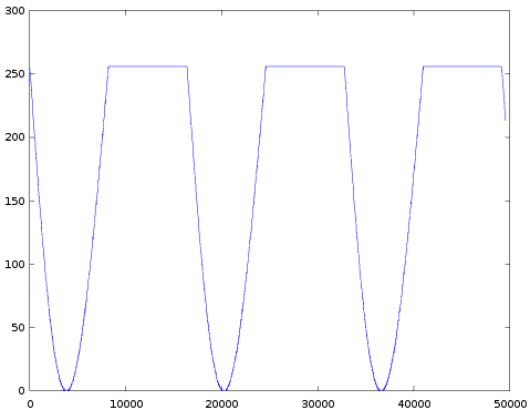
I started the image at the start of the attack phase. So this confirms the first half of the sine wave remains intact and the second half is set to zero.
I've already mentioned this in an earlier post, but here we again see the graph going down instead of up as would be expected for a positive sine wave. But again this is simply because of the measurement setup.
So all this is completely as expected.
Next steps
In the next post I'll probably look at the envelopes again. In particular at the transitions between the different envelope phases (damp, attack, decay, sustain, release). After that I think we're ready to reverse engineer the content of the instrument ROM.
<< YM2413 Reverse Engineering Notes 2015-12-12 | YM2413 Reverse Engineering Notes | YM2413 Reverse Engineering Notes 2015-12-24 >>
