|
|
DevelopmentSega Master System / Mark III / Game Gear |
Home - Forums - Games - Scans - Maps - Cheats - Credits |
YM2413 Reverse engineering notes (2015-03-27)
by andete. Original documents available at: https://github.com/andete/ym2413/tree/master/results
<< YM2413 Reverse Engineering Notes 2015-12-03 | YM2413 Reverse Engineering Notes | YM2413 Reverse Engineering Notes 2015-12-16 >>
Introduction
Last time we looked at how 2 YM2413 operators combined form one channel with frequency modulation. In this post we'll complete that picture and look at the 'feedback' stuff.
The YM2413 application manual contains the following diagram:
                 FB
   <----------(*)------------^
   |                         |
   |  +-------------------+  |  +-------------------+
   |  |           +-----+ |  |  |           +-----+ |
   v----->(+)---->| SIN |---------->(+)---->| SIN |----> F(t)
      |    ^      +-----+ |     |    ^      +-----+ |
      |    |         ^    |     |    |         ^    |
      |    |         | I  |     |    |         | A  |
      | +-----+   +-----+ |     | +-----+   +-----+ |
      | | PG  |   | EG  | |     | | PG  |   | EG  | |
      | +-----+   +-----+ |     | +-----+   +-----+ |
      +-------------------+     +-------------------+
This is much like the diagram in the previous post, with the addition that the output of the modulator operator is looped back to the input of that same operator, so this forms a feedback loop. The feedback signal is still multiplied by a feedback-factor (FB).
Notice how the inside of the operator-block is identical for the modulator and carrier. On the real chip there is also only one instance of this operator. It is time-multiplexed (i.e. reused in sequence over time) for all 18 operators. So it's logical that the operator block has the same features when used as modulator or as carrier.
So from a high level we only need to figure out how the FB-bits (register R#3, bits 2-0) control the feedback factor. Though in practice it's more complicated:
- What are the multiplication factors, more likely it's a shift amount instead of a real multiplication.
- How many bits does the feedback signal have (before and after multiplication).
- The hardware works with discrete instead of continuous values, meaning it takes a small but non-zero amount of time before the output of an operator is calculated, and that calculation is only performed a fixed number of times per second. So the feedback cannot be instantaneous. It's likely that the feedback-input is based on some previously calculated output.
Measurements
We'll investigate the feedback mechanism very much like how we investigated the modulation stuff last time. So let's start by making some measurements. I captured waveforms using the following settings. These are identical to last time's settings, except that now also FB varies:
| Operator | AM | PM | EG | KR | ML | KL | TL | WF | FB | AR | DR | SL | RR |
|---|---|---|---|---|---|---|---|---|---|---|---|---|---|
| modulator | 0 | 0 | 1 | 0 | 00 | 0 | nn | 0 | n | 15 | 00 | 00 | 15 |
| carrier | 0 | 0 | 1 | 0 | 00 | 0 | 0 | 15 | 00 | 00 | 15 |
| reg#0x20 = 0x00 | key-off |
| reg#0x10 = 0x40 | fnum-low=0x40 |
| reg#0x30 = 0x00 | max volume / custom instrument |
| reg#0x20 = 0x10 | key-on / block=0 |
with
- TL varied between 0..63
- FB varied between 0..7
Note that for FB=0 the measurements are identical to those of last time. From this we can already conclude that FB=0 really means no feedback because last time we did not take feedback into account and our model could already 100% predict the measured data.
I did not capture all combinations of TL/FB (that would take way too long). Instead I only measured:
- for TL=63: only FB=7
- for TL=37: FB 0..7
- for TL=0: FB 0..7
You can see the results in the following tables:
One full period
- Modulation depth (TL): 63
| 7 | 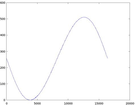 |
- Modulation depth (TL): 37
| +0 | +1 | +2 | +3 | ||
| 0 |  |  |  | 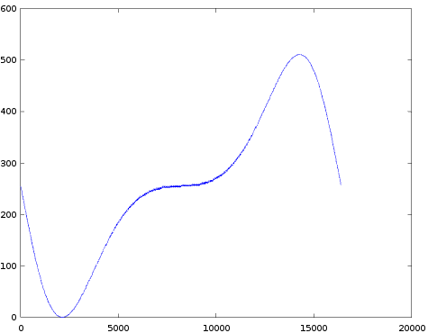 | |
| 4 |  |  |  |  |
- Modulation depth (TL): 0
| +0 | +1 | +2 | +3 | ||
| 0 |  | 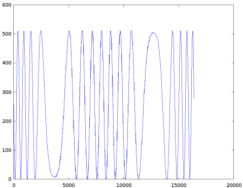 |  |  | |
| 4 |  |  | 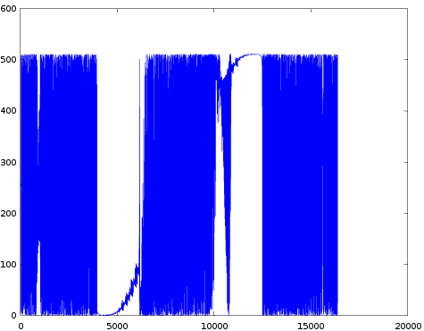 |  |
Zoomed
- Modulation depth (TL): 37, Feeback (FB): 7
|  |  |
- Modulation depth (TL): 0, Feeback (FB): 5
|  |
- Modulation depth (TL): 0, Feeback (FB): 7
|  |
- For TL=63,FB=7 the result is visually not very interesting: it looks identical to last time's graph (for TL=63, FB=0). For this reason I only captured one FB setting for TL=63. If you zoom in closely (not shown) there actually are subtle difference for different FB-levels, more on this later.
- For TL=37 we start (FB=0) with a graph with a 'flat' region (was a popular graph in the last post). When FB increases, the graph evolves towards a more sawtooth like shape. When we zoom in on TL=37, FB=7, we first see the familiar staircase graph, but now with many small 'dense blobs' on it. If we zoom in more on such a 'blob' we see that it consists out of 5 small peaks (3 samples per peak). If you'd zoom in on the TL=63,FB=7 graph (not shown) you'd see similar (but fewer) of these 'blobs'.
- The results for TL=0 are also interesting. For low values of FB (not shown), we see similar small 'blobs' as for TL=37. For FB=5, we start to see regions with much higher amplitude oscillations (image 'fb0-5-zoom.png'). And for FB=6,7 there are regions that are complete chaos (image 'fb0-7-zoom.png'). This is not completely unexpected: positive feedback loops can sometimes be unstable.
Model the observed behavior.
To reverse engineering the feedback behavior, I again took a lazy/smart approach. Instead of trying to figure out everything myself, I first checked what information was already available:
- Next to the diagram at the top of this post, the YM2413 application manual also contains the following table:
    FB (R#3 bits 2-0)|  0  |  1  |  2  |  3  |  4  |  5  |  6  |  7
    -----------------+-----+-----+-----+-----+-----+-----+-----+-----
    Modulation index |  0  |pi/16|pi/8 |pi/4 |pi/2 | pi  | 2pi | 4pi
This confirms that for FB=0 there is no feedback at all. It also shows the amount of feedback increases exponentially with increasing FB register values. This suggests FB controls a shift-amount instead of a (linear) multiplication factor.
- There are two main YM2413 emulation cores, written respectively by Okazaki and Burczynski. Both cores express it in a different way, but they both base the amount of feedback (= input for the modulator operator) on the average of the last two output values of that modulator. So that requires a delay-chain of two(!) output values.
- This forum post by 'carbon14', on Jul 06, 2011 4:21 pm:
http://forums.submarine.org.uk/phpBB/viewtopic.php?f=9&t=1048&start=10
is about feedback on OPL3. It also talks about the sum of the last two samples. Likely in OPLL (=YM2413) it works the same.
With this information in mind and after some iterations I got the following model. (After quite a few iterations actually, because I explicitly also wanted to try (and dismiss) various other alternatives, I won't go into more detail on these alternatives):
uint16_t expTable[256];
void initTables() {
for (int i = 0; i < 256; ++i) {
logsinTable[i] = round(-log2(sin((double(i) + 0.5) * M_PI / 256.0 / 2.0)) * 256.0);
expTable[i] = round((exp2(double(i) / 256.0) - 1.0) * 1024.0);
}
}
uint16_t lookupSin(uint16_t val) {
bool sign = val & 512;
bool mirror = val & 256;
val &= 255;
uint16_t result = logsinTable[mirror ? val ^ 0xFF : val];
if (sign) result |= 0x8000;
return result;
}
int16_t lookupExp(uint16_t val) {
bool sign = val & 0x8000;
int t = (expTable[(val & 0xFF) ^ 0xFF] << 1) | 0x0800;
int result = t >> ((val & 0x7F00) >> 8);
if (sign) result = ~result;
return result;
}
int main() {
initTables();
int16_t p0 = 0;
int16_t p1 = 0;
int TL = 37; // 0..63
int FB = 7; // 0..7
for (int i = 0; i < 16 * 1024; ++i) {
auto f = FB ? (p0 + p1) >> (8 - FB) : 0;
auto s = lookupSin((i - 1) / 16 + f);
auto m = lookupExp(s + 32 * TL) >> 1;
p1 = p0;
p0 = m;
auto s2 = lookupSin(i / 16 + 2 * m);
auto c = lookupExp(s2) >> 4;
cout << 255 - c << endl;
}
}
This model can exactly predict the measured data. Though with these limitations:
- Measurement noise, same as in the previous post. Take a look at this image:

In blue is the measured and in green is the predicted graph for TL=37, FB=7. There's almost no blue in this image, meaning the 2 graphs exactly overlap, including the 'blobs' with rapid oscillations. The only small blue spot is encircled in red, but it's clearly measurement noise (it disappears or moves when re-measuring).
- Different start conditions. This was also already discussed in the previous post: at the very start the attack phase is sometimes (but not always) different than the predictions. Though here, because of the feedback loop, the effect is amplified.
- Another start condition is the value of the two previous modulator outputs. The model initially sets these ('p0' and 'p1') equal to zero. But this might be different from the actual start values. This effect can best be seen in the following image:

Again the measured data is shown in blue and the predicted values in green. There are 3 main parts in this graph, in all 3 parts both curves are chaotic. In the 1st part the blue and green curves are very different. In the 2nd and 3rd part the curves exactly overlap (and are both chaotic). We can better see this by subtracting one curve from the other:

In the first part the difference wildly varies between -512 and 512, meaning the predictions are completely off. In the later parts the difference is zero (actually sometimes +/-1 because of measurement noise), meaning the exact same chaos was produced.
In this mode (TL=0, FB=7) the 'p0' and 'p1' values have a very large effect. So if they are only slightly off, the predicted values will be completely different. But for some reason, after a while, the predicted and actual 'px' values do get in sync with each other, and from that point onwards the model exactly predicts the measurements.
The fact that (after this initial sync problem) this chaos is predicted exactly gives me great confidence that the underlying model is correct. We only need to more accurately set the initial conditions.
Die-shot, feedback
It's always nice to look at the same problem from a few different angles. So let's look at it from a more hardware oriented point of view. What hardware features would be required to implement the feedback mechanism as described above?
Maybe the most obvious feature is the storage for the previous two outputs. So how much storage does that require? One output value (-2047..+2047) requires 12 bits. We store 2 such values for all 9 modulators. So that's 12 x 9 x 2 bits.
Now, guess what I found in the YM2413[1] die-shot:
http://siliconpr0n.org/map/yamaha/fhb013/mz_ns50xu/
Vertically near the top, horizontally in the center, there are two blocks close to each other, each containing 12 rows of 9 bits arranged in a shift register. That's exactly what we need here. So this again increases my confidence in the model.
Die-shot, summary
In the previous posts I already identified other regions in this die-shot. Let's repeat/summarize that information here. Take a look at this annotated image. (It's a snapshot generated from the link above, I manually added the colored annotations. Though I still suggest to actually visit that link because it allows to freely zoom/pan the image in much more detail):

- 'FB' region marked in red: that's the storage for the feedback feature we talked about above. It contains 2 x 9 x 12 bits.
- 'PG' region marked in green: 18 x 19 bits. Stores the 10.9 bits fixed point phase counter for each operator.
- 'EG' region marked in yellow: 18 x 7 bits. Stores the envelope counter for each operator.
- 'REG' region marked in orange. Contains 9x7 + 9x7 + 9x4 + 9x4 bits. This maps on the 9 x 22 bits required to store registers R#10-R#3F. More in detail: registers R#10-R#18 (8 bits), R#20-R#28 (6 bits) and R#30-R#38 (8 bits).
- 'INSTR' region marked in white. This is the instrument ROM + decoder, it likely includes storage for the custom instrument (registers R#00-R#07, 63 bits).
- 'SIN' region marked in purple. This is the log-sine table plus decoding logic.
- 'EXP' region marked in cyan. This is the exponential table plus decoding logic.
- 'DAC' region marked in blue. This is the 9-bit DAC (2D-array of 16x32 switches, plus 4-bit and 5-bit temperature decoders).
With this all the major areas containing storage are identified. The remaining minor bits that I can identify are (though still very much speculation at this point):
- Near the yellow EG region there are 3 chains of 18(?) bits (though only 16 bits are clearly visible, perhaps the other 2 bits are interwoven with the rest of the logic). Possibly these bits are used to store the envelope phase per operator (damp, attack, decay, sustain, release).
- Right from the green PG area, in the top right corner is 1 chain of 15 bits. No idea yet what this is. Perhaps this is the shift register for the LFSR random generator for the rhythm instruments (though the Burczynski emulation code uses a 22-bit shift register).
- Below the blue DAC region are 9 chains of 5 bits. Perhaps these are used to temporary store the (9-bit) DAC output value and repeat it at some later time. The YM2413 application manual does say the (5) rhythm channels are output twice in each 72 clock-cycle period.
There must also be a 'global counter' somewhere that controls the envelopes and the LFO AM and PM stuff, I did not yet find it (though it's not a shift register, so I don't recognize it). I also didn't calculate yet how many bits this counter requires.
The other area is mostly filled with logic functions(*). I can sort-of recognize adders, but the other logic components remain a mystery to me.
(*) Actually most area is filled with wires instead of logic. But it's easy enough to distinguish between the two.
Next steps
Not sure yet. I think all major components have been looked at. Maybe I should go over all previous posts and tie up some loose ends? Or maybe I should go over the YM2413 registers and check whether all bits have been covered?
Some of the bigger remaining TODOs are:
- Investigate the transitions (e.g. key-off -> key-on transition and the envelope transitions it triggers).
- Reverse engineer the values from the instrument ROM.
- Investigate the rhythm sounds.
<< YM2413 Reverse Engineering Notes 2015-12-03 | YM2413 Reverse Engineering Notes | YM2413 Reverse Engineering Notes 2015-12-16 >>
