|
|
ForumsSega Master System / Mark III / Game GearSG-1000 / SC-3000 / SF-7000 / OMV |
Home - Forums - Games - Scans - Maps - Cheats - Credits Music - Videos - Development - Hacks - Translations - Homebrew |
View topic - Game Gear Rom Paging Chip
 |
Goto page Previous 1, 2, 3 |
| Author | Message |
|---|---|
|
|
- Interesting.... I've never come across that term. I realize that it meant to prevent an output from activating, but never heard it described as the "inverse" of Enable specifically. It was probably the digital electronics lecture I missed on a sick day or spent it on the side of the road changing a flat tire in the rain. :( So.... good to know.
Ahh yes, I actually soldered a line from the CPLD to the cartridge edge. The /RESET line is not used on my SMS cart design, so there was no trace for it. I'll double check that regardless.
This is also good to know. :)
That's a really good point. Thanks for the tip. I'll swap those lines up to 22 AWG wire. Thanks viletim....I'll start with the smaller ROM file too. Great advice all around. Thanks again. -Gerry |
|
|
|
|
|
|
|
I've been looking at this design and the CPLD design by Viletim and I notice his design utilises a reset signal to clear\preset the values in the flipflops when the console is powered on.
However, this design uses the 74x574 which does not have a reset\clear function. Is it possible that random values loaded into the 574s at power on could cause incorrect data on the EEPROM address lines, and the console's inability to actually read out the correct data to initialise the game? |
|
|
|
|
|
|
|
It's not only possible, but extremely likely. However, I had a talk with Maxim previously and he told me that GG/SMS's built-in ROM pre-loads the three FCRs with the corresponding values 0, 1 and 2 (for each page).
So, there is no need to worry about that initial FCR "garbage". Kind regards, CK |
|
|
|
|
|
|
| Did I? I was wrong - most SMS1s' BIOSes don't (and as a result can't play 4Mbit TecToy games), and many GGs have no BIOS and boot to the game directly. | |
|
|
|
|
|
So the lack of power-on reset could be a problem? |
|
|
|
|
|
|
| On the hardware I mentioned, yes. | |
|
|
|
|
|
| Would that include the SMS2? (that's the only system I have) or does it have a BIOS that can reset the registers itself? | |
|
|
|
|
|
| That should be OK. | |
|
|
|
|
|
|
I'm back on this again (amazing, I know) Hope you guys are still here looking at this...
Now that I got my SMSReader working (1 missing connection to /M0-7 line) I retested your cartridge design and guess what - it works! Using a 2Mbit chip (W29C020) the SMSReader managed to read the ROM fine with both autodetect and manually selecting 256K. Still doesn't work in the SMS itself, though, and 2Mbit is all I tried so far with a ROM of 'Sonic the Hedgehog' I guess the SMSReader uses a different method of accessing the cartridge? Or maybe it is not as fast as the SMS and there is a signal integrity problem? I will try other ROM sizes and see what happens, but for now I guess it's good news - something is in fact working! |
|
|
|
|
|
|
|
Thanks Agent24. Those are excellent news, believe me!
I abandoned this project as I got the feeling that the diagram was wrong and had no resources to test my theory. Yes because this schematic was just theory. I designed it hoping that someone in the future would use it :) Your SMSReader uses the SMS's paging scheme, implemented in the mapping circuit, so it's natural that it worked! Honestly, for it not to work on real Sega hardware must be because of some wrong/missing signal or because of uninitialized FCRs. Does SMSReader initialize any FCR before starting rolling down the memory addresses? |
|
|
|
|
|
|
| Looking at the source (last touched 6 years ago), it looks like it writes to $fffc (to select ROM) and $ffff (or $8000) only, when dumping larger ROMs. That's assuming you're referring to my software; the hardware does nothing. | |
|
|
|
|
|
|
If the SMSReader doesn't clear the FCRs why does it work?
I bought one of those cheap logic analysers on eBay, when I get it maybe I can figure out what's going on. |
|
|
|
|
|
|
| It writes to any FCRs affecting the addresses it will read from, unless it is dumping a small ROM, in which case it assumes there are none. | |
|
|
|
|
|
| Got the LA (one of those LCSoft boards), now I just have to figure out how to use Sigrok... | |
|
|
|
|
|
|
Sigrok looks good, even has a decoder for Z80 which might be useful. Problem is the LCSoft board appears to only accepts 3.3v inputs so I need to make an input board: http://sigrok.org/wiki/Circuits_for_barebone_boards
Will update later... |
|
|
|
|
|
|
| Almost finished with getting this thing up to scratch... then I should be able to test it.. hopefully it's fast enough...wish I had a proper DSO.. :( | |
|
|
|
|
|
|
Got the board done last night (fun SMD soldering!) and now have the latest version of Sigrok. Did a basic test and all inputs seem fine with a square wave coming from an Arduino.
Now I just have to figure out what I should be checking on this cart! I guess I should start with taking some dumps through the SMSReader since that works, and compare things between that and in the actual SMS, see what is different. |
|
|
|
|
|
|
|
Just had some fun with this and Sigrok...
I was going to try testing between SMSReader and SMS2 to see differences, problem is it's *completely* different. Also the SMSReader is a lot slower... Anyway, I checked the theory to see if the FCRs were outputting garbage, what was interesting is that they don't seem to output anything at all. To start with, I looked at FCR0 (U1) and checked its inputs. There seems to be no clock input, Which appears to be because U4B is doing nothing - the outputs stay high, Which appears to be because U4B never gets an "Output enable" signal, Which appears to be because U7A never gets an input pattern of all highs at any point. Clearly the design *works* - on the SMSReader at least. I wonder if the problem is that the SMS itself, being much faster, is causing signal integrity problems or perhaps some of these chips are too slow, and signal propagation is affected to the extent that it buggers up the timing? Either way, without knowing what I'm *supposed* to see, I don't really know what's going on. IIRC, you said you were able to do a simulation in Multisim - did you load a ROM file somehow? Were you ever able to get a timing diagram? Would there be any way to run the SMS BIOS code in some simulation and compare that with the captures? Might try building the CPLD cartridge and comparing, although without access to the internal logic there is probably not much to gain from doing that! I have attached some Sigrok capture files. You can view them in Pulseview in Linux or Windows (sigrok.org/wiki/Windows) If you view them, it may help to know that the point where the A14-A17 lines on the ROM side go low is the point just when Alex Kidd pops up on the screen... |
|
|
|
|
|
|
|
Well. It's been a while(!), but I just built up a copy of Viletim's CPLD cartridge complete with RAM and backup battery etc. I have only tested Sonic the Hedgehog so far but it seems to work. Funny though the SMSReader does not autodetect the cartridge size, but does dump correctly if I select the size manually. I suppose because the design is "universal" it cannot really be expected to autodetect.
I still want to get the other mapper circuit working if I can, though, so I'll start playing around with it some more and see what happens. Perhaps I can compare things between the two cartridges and see if I can figure out what's going wrong with it. Just wanted to say I haven't forgotten about it... |
|
|
|
|
|
|
| SMS Reader autodetects by looking for mirroring and then also by removing trailing blanks. If the upper memory area is not a copy or blank then it won't work. | |
|
|
|
|
|
|
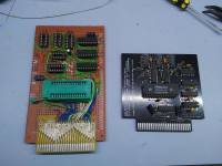
I decided to try running this circuit on the board that I built for Viletim's mapper, to see what happens.
I worked backwards from his design, removing/changing each section to function as in this circuit, until it stopped working. The difference between it working and not working, seems to be that his mapper initialises two of his FCRs (bank 1 and bank 2) with certain data at power-on-reset. (Bank 1 has the A14 line preset HIGH, Bank 2 the A15 line HIGH.) I don't know why, and if the SMS2 BIOS is supposed to initialise the FCRs itself then this seems unnecessary. (This happens only when set to SEGA mode, not CodeMasters) BUT, if I remove that data preload function, it always boots the BIOS and ignores the cartridge as if it's not even there. Whether adding this feature will allow the discrete-logic version to function, I am not sure, as my previous test with the logic analyser seemed to conclude that the SMS was never writing anything to the FCRs at all, but maybe that's the problem. However, without knowing exactly what the BIOS actually does, step by step, from power up, I can only guess things. If this is indeed the reason, I should be able to add a dual-D flip-flop to allow for preloading of those specific bits. Otherwise, if it's a logic timing/signal integrity issue, it might still never work. But I suppose it's worth a try. |
|
|
|
|
|
|
|
I have updated the design to add the FCR reset and preload function, as well as worked out a PCB layout, in case the breadboard approach was also causing problems.
Will be sending off the design to get some custom PCBs. Would have made it myself as I do normally but to keep everything compact and routable I needed to use VIAs and PTHs. If it works I'll update it to support larger ROMs (only wired up for 2Mbit support at the moment) etc. |
|
|
|
|
|
Last edited by kejoxen on Tue Mar 19, 2019 8:35 am; edited 1 time in total |
| I've been following this post for a while, thought you had given up, can you post some pictures please? | |
|
|
|
|
|
It went on hold, life happened, and I didn't have any real way to troubleshoot the design, until I built that CPLD based cartridge and was able to play around with various concepts. Nothing to see yet - I just sent the Gerbers to JLCPCB, I should get the boards in a week or so to test my design changes and theory. Bear in mind if it makes no sign of improving I really don't know what else to try. The logic that I've just implemented in 7400 chips worked in the CPLD but of course there will be differences, namely much better signal integrity, faster gates, lower propagation delays etc. The original Sega mappers were all made in an ASIC. It may be that a discrete design just isn't possible - that things aren't fast enough when done that way, or something. In any case, if you want something to play around with in the mean time, I'd recommend Viletim's CPLD design. It seems to work pretty well! You can see some pictures of what I've done with that in the thread here: http://www.smspower.org/forums/9821-CPLDPagingICMapper |
|
|
|
|
|
|
|
Finally, some progress!
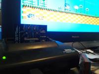
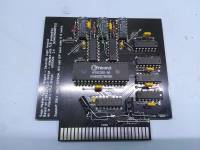
I received the PCBs yesterday, and assembled one today. It turns out there were a couple of minor issues. The first is that I miscalculated the size of the ZIF socket, and wasn't able to install it for the EEPROM. I had to use a standard socket instead. Not a big deal as it's only a prototype. Then I put the card into the SMS and got ... Software Error - which wasn't what I'd hoped for - but which was a big improvement upon last time, where it did absolutely nothing. Then, I put the new design into the SMSReader and did a dump. It did auto-detect the size OK, but the dump was bad. I loaded the original ROM and the bad dump, and compared in a Hex editor. It quickly became apparent that while the data was uncorrupted, there was some issue with the bank switching. The second 32k of data was identical to the first. That is to say, the data from 0x0000-0x7FFF was correct in both dumps, but on the bad dump, the data from 0x8000-0xFFFF was the same as the data in 0x0000-0x7FFF. This pattern became apparent throughout the dump. Every second 32k block mirrored the one before it. So 0x10000-17FFF also mirrored 0x18000-0x1FFFF, and so on. It was quickly obvious that there was an issue with the A15 address line to the EEPROM - i.e. it was never going high. I went back to the schematic and discovered I had made a typo on the net name, and the A15Out line from FCR2 was connected to nothing, when it should have gone to the EEPROMs A15 pin. After adding a wire to connect the correct pins, I was able to get a verified dump. Then, the moment of truth - I put the board back in my SMS and powered it up .... the SEGA logo came straight up ... waited a few moments... and suddenly - Sonic the Hedgehog began running! So far it's been working great - I played through until I wiped out on Jungle Stage 1 - but there were no issues that I could see. So it seems that this design does in fact solve the problems present in the previous one. There is still work to be done... At the moment this design only supports 2MBit EEPROMs and only a certain EEPROM pinout. It also only works as SEGA compatible due to the FCR data preloading. There would need to be extra circuitry added to toggle this feature when running the Codemasters style mapper etc, as in Viletim's CPLD design. I think it will be possible to make a more fully-featured design, but there will need to be more ICs added. At the moment there are 11 ICs including the EEPROM. It may well need 20+ (!) to make a "universal" mapper with 7400 series ICs. So again, a CPLD/FGPA etc version is probably more sensible. But... this one is easy(er) to source and build. Theoretically. I do have 4x spare PCBs if people want them... (not much use to me, I'll be updating the design soon) but bear in mind they do have limitations and errors!! 1) You will need to run a wire from U6 Pin 6 over to either U7 Pin 4 or U11 Pin 3 to fix the missing A15 line. 2) You also can't use a ZIF socket as there isn't enough room (unless perhaps you mounted U1 and U6 from the rear of the board - bend the pins backwards!) 3) You may also want to file/sand the connector edge of the board to a chamfer. This would avoid the spring contacts in the slot connector from potentially being squashed (not fun). In any case, this version's BOM is as follows: 3x 10k resistors 10x 100nF ceramic capacitors 2x 4.7uF 10v or higher electrolytics 1x W29C020 or equivalent 2Mbit EEPROM 1x 74x133 1x 74x74 1x 74x139 1x 74x125 1x 74x20 2x 74x04 3x 74x173 9x wire links 74HCT series are probably best, but mine has a mixture of HCT, ALS and LS parts. Original 1970s era 7400 parts may or may not work, especially for gates with longer propagation delays to start with such as the 74133. 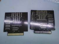
|
|
|
|
|
Goto page Previous 1, 2, 3 |