|
|
DevelopmentSega Master System / Mark III / Game Gear |
Home - Forums - Games - Scans - Maps - Cheats - Credits |
YM 2413 Reverse Engineering Notes 2015 - 03 - 05
by andete. Original documents available at: https://github.com/andete/ym2413/tree/master/results
<< YM2413 Reverse Engineering Notes 2015-02-09 | YM2413 Reverse Engineering Notes | YM2413 Reverse Engineering Notes 2015-03-11 >>
This is a follow-up on 20150209.txt. My first idea was to write a single document and update it each time I figure out more details of the YM2413. Now I feel more like writing several short texts and only at the very end condense everything into one final document. I'm not sure yet what's best. The advantage of this new approach is that I can more easily point out mistakes in my earlier findings.
So let's start with a mistake from the previous text:
The goal of the previous text was to map measured ADC levels (12-bit) back to YM2413 levels (9-bit). I measured a sine wave, calculated the histogram and did peak detection on that histogram. I found that the distances between consecutive peaks was not constant and assumed this was caused by measurement noise and therefor applied a smoothing algorithm. It turns out this assumption was not completely true ... I'll come back to this.
In the mean time I was pointed to this picture: http://siliconpr0n.org/map/yamaha/fhb013/mz_ns50xu/ This is a die-shot of the YM2413[1]. Personally I can't make much of this picture. But I have a friend who (used to) design digital/analog ICs at the transistor level (so more or less manually draw these structures). And together we could derive some interesting properties from this picture.
We mostly looked at the DAC, this is the first larger rectangle in the top-left corner. If you zoom in, you see 512 switches arranged in a 32x16 grid (personally I only see crossing wires instead of switches). This is a thermometer-coded 9-bit DAC, left from the switch-matrix is a 4-bit thermometer-decoder that selects the columns and right there's a 5-bit thermometer-decoder to select the rows.
You can also see two wires that go from the bottom center of the switch matrix to the top-left. These are the signals that direct the output of the DAC to the RO or the MO output pins. The RO/MO pins are the 2 leftmost pins located at the top row.
Because of the 32x16 arrangement of this DAC (and because, I'm told, this is a relatively cheap low-quality implementation), it's not unexpected to see this 32x16 structure in the DAC output levels. Looking back at the 'displacement.png' image of the previous text (this diagram can more or less be interpreted as a measure for how much the DAC output deviates from a perfectly linear output), you can actually see this 32x16 structure a bit. With some goodwill you can see 'regular' peaks that repeat every 32 steps (and between the peaks the curve should linearly decrease, though this feature mostly drowns in the noise). This curve is closely related to the INL/DNL curves of a DAC (see https://en.wikipedia.org/wiki/Differential_nonlinearity). And for this type of DAC, that curve is expected to show a saw-tooth shape.
Anyway, the conclusion is that the smoothing step I performed last time is actually counter-productive because it hides the inherent non-linearities of the YM2413 DAC. (But as I mentioned last time, the smoothing step did not have that much effect in practice anyway).
Another big change compared to last time is that I now perform 16x oversampling when capturing the YM2413 output signal. That is instead of sampling each YM2413 value once we take 16 samples (shortly after each other in time) and sum these 16 values. This results in a much less noisy signal. The SoC we use has hardware support for oversampling.
Our ADC returns a 12-bit value. If we sum 16 such values we obtain a value that has 12+log2(16)=16 bits. So from now on, depending on the context, I'll report ADC measurements as either 12-bit or 16-bit values. In theory, assuming we have Gaussian white noise, 16x oversampling increases the effective resolution by a factor sqrt(16). That would mean we now have an effective ADC resolution of 14-bit. I don't know to what degree the condition of Gaussian white-noise holds in this situation.
The disadvantage of 16x oversampling is that it takes 16x longer to execute. So I also had to clock the YM2413 16x slower. The YM2413 is now running at 50kHz. That's a lot slower than the 3.5MHz the YM2413 was designed for. (From the die shot we could derive that the output of this type of DAC remains stable even if you heavily under-clock the IC, and the measurements confirm this, so from that point of view there's no problem). Unfortunately that also means that sampling a YM2413 sound that would normally take 1 second now takes over 1 minute.
As I mentioned before, the main reason for oversampling is to reduce the noise of the measured signal. Though even now the signal is not yet perfect, so occasional misclassification is still possible. I also tried higher oversampling factors (32x, or even 256x) but that didn't seem to improve the result any further.
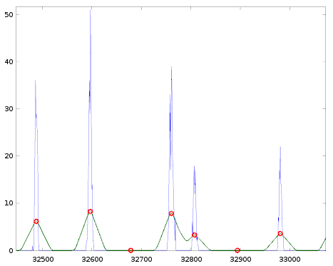
The result can be seen in the following image:

This shows a (very) small portion of the histogram of a sampled sine wave (see previous text for a lot more detailed description). The blue line is the actual histogram. The green line is a smoothed version of the histogram (I used a simple triangular shaped smoothing window) and the red dots are the estimated peaks.
I've intentionally shown one of the noisier parts of the histogram (the leftmost side of the histogram, corresponding to the highest amplitude YM2413 outputs). You can see that there are still samples that lie almost halfway between two peaks. But it's better than our earlier results (without oversampling). Also note that the horizontal scale is 16x larger now and in the vertical direction the peaks are lower because the sample values are now spread over more bins.
The following image shows the center part of the histogram:
As expected there are missing peaks in this histogram (see previous text). The detection algorithm tries to guess the locations of such missing peaks, that's why there are also a red dots for those 'peaks'. Near the center there is *significantly* less noise compared to the edges of the histogram (the center corresponds to the lowest amplitude YM2413 outputs). In the center we can very clearly see distinct peaks.
One really interesting feature in the above picture occurs near the very center (near x-value 32768). There we very clearly see two peaks, but these are much closer together than all the other peaks. In the old measurements (without oversampling) the horizontal resolution was not high enough to distinguish these two peaks[2], so they were counted as a single peak. Because of this I wrongly reported the YM2413 only outputs 511 distinct values. But now when counting all peaks (including the missing ones) we do see 512 distinct peaks.
I'm not sure yet what this dual central peak means in terms of emulation. It's neither correct to model this as 511 or 512 peaks because the distance between the two center peaks is smaller compared to all the other peaks. For now I think I'll treat this as '+0' and '-0' and map them both on the same '0' output value (thus effectively use only 511 distinct output values). Later I'd like to revisit this, maybe by studying the die shot again and try to figure out how an ideal circuit would behave. In a way this is similar to the non-linearities in the YM2413 DAC. Because of slight variations in the fabrication process, different YM2413 chips will have a slightly different DAC characteristic. We emulate this as an idealized DAC that is perfectly linear. It might be possible that the position of '+0' and '-0' also varies between different chips and that in an ideal chip they both coincide. But at this points that's only speculation.
The last thing I'd like to mention in this text is the new code I've written for the ARM SoC. Before when I wanted to run a different test, I had to re-flash the ARM with a new program. Now I've written one program that accepts instructions over USB (and also send back results over USB). These instructions can start/stop YM2413-output-capturing or write YM2413 registers (and debug commands to toggle LEDs or echo data).
This should allow to in the future more easily capture various YM2413 signals. E.g. play a sine wave at various different volumes and/or different frequencies. That'll be my next step.
- ^ Actually the FHB013
- ^ In retrospect when looking back at the old (non-oversampled) data, this 'dual' peak was actually somewhat visible. Though it only showed up a as an asymmetric broader peak with a slight dip between the left and right side. At the time I dismissed it as measurement noise (because other peaks sometimes also showed such dips).
<< YM2413 Reverse Engineering Notes 2015-02-09 | YM2413 Reverse Engineering Notes | YM2413 Reverse Engineering Notes 2015-03-11 >>
