|
|
ForumsSega Master System / Mark III / Game GearSG-1000 / SC-3000 / SF-7000 / OMV |
Home - Forums - Games - Scans - Maps - Cheats - Credits Music - Videos - Development - Hacks - Translations - Homebrew |
View topic - Simplest SEGA Mapper with off the shelf parts.
 |
| Author | Message |
|---|---|
|
Simplest SEGA Mapper with off the shelf parts.
|
|
I've reworked my current mapper replacing the ATF16V8 PLDs, which require a dedicated programmer and are pretty much obsoleted, with a 512K Flash ROM that anyone can even order pre-programmed from some vendors (like Microchipdirect).
In essence the mapper needs the Flash ROM programmed with the attached .bin file, 5 10K resistors and 1 or 2 74HC573 latches, the circuit is as follows: 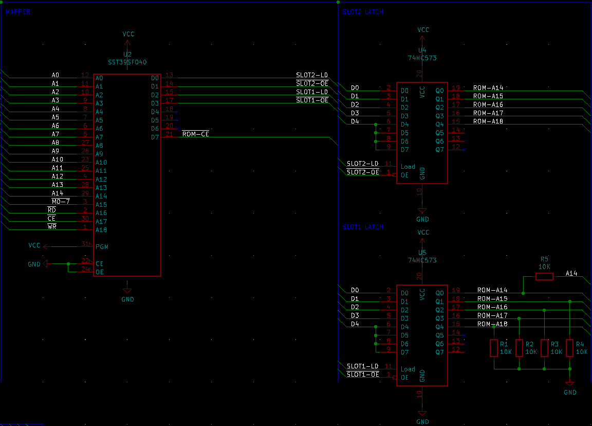
Connect the game ROM to the mapper as follows: Game ROM Mapper A14 ROM-A14 A15 ROM-A15 A16 ROM-A16 A17 ROM-A17 A18 ROM-A18 !CE !ROM_CE Connect the rest of the game ROM pins to the SMS slot like a regular ROM. I've ordered a few boards with this design. Further testing of this mapper required but it seems to work. 
|
|
|
|
|
|
|
| Thats a cleaver approach. I like that! | |
|
|
|
|
|
|
Would you mind explaining how are you using a ROM as a mapper?
Thanks! :) |
|
|
|
|
|
|
From the SST39SF040 datasheet there is an option to drive the Data bus via changes on the Address bus without resetting !CE or !OE, making the ROM (chronogram on page 14) into an asynchronous programmable combinatorial circuit. Also, is not the rom by itself doing all the work. You need the latch circuits and some pull-downs as well. The ROM just controls when to update and activate the address latches. |
|
|
|
|
|
|
| Brilliant! I was analising your code, and thinking about implement on-cartridge RAM. | |
|
|
|
|
|
|
Perfect!! You're the man! I started a post on this without looking through the forum first!
Have you done any further testing since the post? I want to bootleg some exotic games like SORII and other large 512kb ROMS.. would this support? |
|
|
|
|
|
|
|
That's pretty interesting.
It raised a doubt I have for years and think that's the perfect occasion to ask: Do we really need to decode the full address bus? I mean, does any game assert the cartridge's /CE and /WE on other addresses that are not mapper related? |
|
|
|
|
|
|
|
Games that use the 3D glasses write to the region at $FFF8-$FFFB, so you need to include A2 at least.
I helped design a mapper replacement that ignores A9-A3 and it seems to work ok. (i.e. writes to $FC00-$FFF7 would be problematic but apparently don't happen) |
|
|
|
|
|
|
|
I've ordered ST M27C4001-10F1 4mbit EPROMS (for master system ROM) + the SST39FS040 for your Mapper here.
Planning on throwing a PCB together later, should squeeze into a shell. Just confused on when you would need 1 or 2 latches, it doesn't make sense to me having everything doubled up on a bus for the input and output? If anyone can point me in the right direction, I will make the board as per schematic, with only 1 requiring the external components? |
|
|
|
|
|
|
|
Also the 10k resistor on A14 latch 1, where's that going? is that a pull up?
** sorry didn't look properly, just another pull down You can use a resistor array bus but the ones with common on pin 6 containing 5 resistors seem to be out of stock everywhere. If i find one i will paste it here ** 4306R-101-103LF. |
|
|
|
|
|
|
The standard SMS mapper effectively has two¹ movable windows, for access to memory when the Z80 is accessing $4000-$7FFF, or $8000-$BFFF. The bottom 16KB effectively always accesses the first 16KB of the external ROM, and the last 16KB effectively always accesses the SMS's built-in 8KB of RAM. So there are two latches to hold each of these. The trick here is that the two latches' have "output enable" pins. These can be selectively enabled so that only one, the other, or the pull-down resistors, selects which region of the ROM is accessed by the Z80. This is very similar to the NES mapper used for the unlicensed game Impossible Mission 2, where two latches are used in the same way to increase graphics diversity. ¹Pedantically there's a third window, accessible at $0400-$3FFF. Almost no games use it. |
|
|
|
|
|
|
Thanks for that. Is there a simplified way to determine which games require one or both latches? |
|
|
|
|
|
|
To the best of my knowledge, most games seem to use both. You could use MEKA's debugger to find which ones write multiple different values. However, trying to optimize this is really the wrong place: the ROM is much more expensive than the latches are. |
|
|
|
|
|
|
|
That's interesting.
Maybe the decoding can be done with a 74'139 if you won't be using the 3D glasses. About the Codemasters mapper, is it me or it's very similar to NES' UNROM? |
|
|
|
|
|
Last edited by lidnariq on Tue Jul 06, 2021 12:33 am; edited 1 time in total |
You'd need to make sure that the register doesn't overlap with SMS-internal RAM, so you have to make sure A13 is high. But you're right that you might be able to get away with much less complete decoding. A 74'138 might be good enough, checking /MREQ, A13, A2, A1, A0, /WR. And a separate 74'139 to decode the latch /OEs. (edit: remove nonsense) The "one fixed bank" and "one movable bank" seems to be ubiquitous. I've seen it in a lot of more-modern embedded systems too. |
|
|
|
|
|
|
|
Ok guys, made a start
This wasn't done carefully and the readability isn't the greatest but should be good so far. will use a ~1k resistor to tie the unused address lines on the mapper high, all other unused lines directly to ground. 4 x 0805 caps should suffice for AC shunting/ cleaning up the power. Should just be a matter of the 50 pin edge connector being added then all the labeling done. If you see any mistakes give me a heads up, and of course I will credit the author. no rush on the PCB :) I can see the mistakes on the BUS for slot 1 and 2 OE etc, just squeezed this in between errands and cloning across drives for my main, stuck on a lappy 
|
|
|
|
|
|
|
|
Looks like a very nice design!
Thanks for sharing. :-) I've seen a bootleg cart that used a "sanded" IC and 2x 74LS670. Not sure if the full mapping with SRAM control was implemented, but would be nice if the sanded IC could be identified. Probably it's some kind of PAL or GAL... I'll try to get pictures of it if it ever comes to my hands again. |
|
|
|
|
|
|
|
Does anyone know how to add BATTERY save to this schematic?
haven't gone back to the PCB design yet, being using after burners/ golden axe etc... and now very interested in a copy of Monopoly we have. Found someone that turned that into a retranslation of Phantasy star with no issues. Just wondering how to add save functionality to this. |
|
|
|
|
|
|
You'll need to add another latch, and also have to give up on fully decoding the address bus - the 512KB ROM-as-PLA doesn't have any more inputs, and you need to change the logic depending on what the output of the latch is. See: https://www.smspower.org/Development/Mappers#TheSegaMapper Currently, the two latches on this board are instructed to latch the data bus on a write to $FFFE or $FFFF. The new latch will need to latch a write to $FFFC, but will only care about D3. The output of that latch will need to go back to the ROM, and one of the three unused outputs from the ROM will need to go to /RAM-CE. The contents of the ROM-as-PLA will also need to change. |
|
|
|
|
|
|
|
Thanks Lidnariq. Won't be any room though.. I suspect you'd only jusssst manage to squeeze this into a shell as is... Maybe tracking down well priced monopoly copies to turn into games with save functionality is the best route. There's a gamegear conversion of a really well made RPG from 1995 that I have my eye on...
Mind you an everdrive IS available but lacks that authentic feel lol |
|
|
|
|
|
|
|
Hello, been lurking on the forum for a long time, decided to finally register an account.
Has anybody tested this mapper in real hardware? I'm considering making a cart for personal use using it, I can share the schematics and PCB design after its done if it is of interest of you guys and NeonMan permits me. |
|
|
|
|
|
|
|
I have made a slight redesign of @NeonMan's circuit. It basically adds a third latch and uses all bits in the latches in order to select from many 512KB ROMs.
If the memories used were through hole, a new, enlarged case would need to be designed. Alternatively, if everything was built with surface mounted components the reclaimed space may be enough to fit into a standard cartridge. Initially, I thought on adding the third latch for the 0x0400-0x3FFF space but I think it may be repurposed. I mainly have checked the ROM space documentation and still haven't revised the documentation for cartridge RAM. In case such functionality was to be enabled, what more steps should be needed? Thank you in advance |
|
|
|
|
|
|
|
This morning I have made a revision and therefore corrected several errors found in the first redesign I posted. At the same time, I designed the cartridge interface and separated the circuit in three separate sections: the interface, which consists in the cartridge connector plus buffers for data and address; the mapper, which contains the banking mechanism; and finally the memory bank, which contains a set of 512KB memories.
As for changes over the original design of @NeonMan, I ceased to use the #M0-7 signal and used A15 instead. To make sure it was a memory transaction I tied the #MemRQ signal to the memory acting as mapper and added resistor packs to add some sort of "default" state. This grants control over the whole memory range visible to the Z80. I would like to know what do you think about it - I am of the doctrine that there's always room for improvement. Thank you in advance |
|
|
|
|
|
|
|
Today I have done a redrawing from scratch. Instead of using 512KB memories, I have redrawn it to use larger memories, At the same time used the third latch as the cartridge RAM enable, using the extra pin on the ROMs to switch logic.
RAM is implemented using ferromagnetic memory. This means battery-backed cartridges not only can be implemented but wouldn't need the battery at all.The cost is the usage of the #refresh signal to strobe the address. I have measured the free space in the cartridge and found that it can be actually implemented in a compatible case of the same size as the originals from Sega. The price to pay is the usage of SMD components. 
I don't see why 27C080 couldn't be used in a prototyping batch and cheaper flash memories once an esay way of programming them is found. Again, I would like to hear about your feedback, please. Thank you in advance. 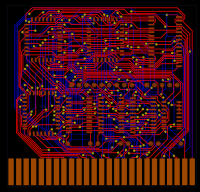
|
|
|
|
|
|
Simplest SEGA Mapper with off the shelf parts.
|
|
I haven’t looked at your schematic but I noticed a couple of things on your board layout:
There are no screw holes. Did you omit those on purpose? There’s no ground plane? Or thick power rail? Some of the ICs are very close together, maybe 2mm apart. SMD that close are a bit of a pain to solder and desolder. |
|
|
|
|
|
|
This is my first SMD design. For this reason I expected flaws in the design. When designing in THT I do know what is the width of the rail, but in SMD I am not aware of the recommended one. The layout is not definitive, I did it only to test if it just had any connectivity problems between the components. I take notice about the spacing. About the holes, they need to be added. I would need a reference about their placement on official cartridges (not saying that there aren't, just that I don't find them). In any case, thank you very much! |
|
|
|
|
|
|
|
I might be missing something, but feels like you don't need the 139.
The combinatorial ROM computes /ROMCS, /FFFF_RD and /FFFE_RD, and each is only consumed in one place, with all three going into the 139 so surely you can reprogram it to output a signal like /ROMCS which goes to /CE of both game ROMs and then put B6 and B7 directly into the /OE pins? Also, I know they are smaller (less capacious), but SST39SF040s are *much* cheaper than AT27C080 and if you use small SMDs you might find you can put four SSTs on there for a third of the price of two ATs. |
|
|
|
|
|
|
You have a point here. The cost of building this cartridge would scare many. About the decoder, if the image to be burnt exceeds the capacity of the ROM, then would need to be selected by the bank address registers in addition to the #ROMSEL. |
|
|
|
|
|
|
Maybe I'm misunderstanding - are you planning for it to be expandable to up to 4MB? If so, then the line decoder makes sense, but if that's not the idea then isn't it easier to just, say, ignore bit 7, mirror the ROM and save yourself the board real estate currently given up to the 139? |
|
|
|
|
|
|
Yes, that's exactly the idea. :) But I guess I could simplify it and leave it mirrored. 512KB is not a small size for a Master System. |
|
|
|
|
|
|
Well you have 2MB right now with the two AT27C080s don't you, so that's certainly not small for SMS! |
|
|
|
|