|
|
ForumsSega Master System / Mark III / Game GearSG-1000 / SC-3000 / SF-7000 / OMV |
Home - Forums - Games - Scans - Maps - Cheats - Credits Music - Videos - Development - Hacks - Translations - Homebrew |
View topic - Power Base Converter info
 |
| Author | Message |
|---|---|
|
Power Base Converter info
Last edited by Charles MacDonald on Thu Feb 18, 2016 5:44 pm; edited 1 time in total |
|
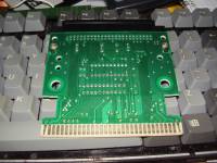
The Power Base Converter has a 315-5342 custom chip. This chip is a Signetics PLS153 programmable logic array which implements user-defined combinatorial logic. I've always been curious what this is used for when other third-party adapters have no extra hardware.
Thanks to Smitdogg from the Dumping Union, we got a good read of the chip and I converted the JEDEC fusemap into logic equations. The chip is programmed to store eight bytes of ROM data, with the first 6 used: 21 01 E1 : LD HL, $E101
25 -- -- : DEC H F9 -- -- : LD SP,HL C7 -- -- : RST $00 01 01 -- : LD BC, $xx01 This fragment of code initializes the stack pointer because the Genesis has no BIOS and the stack pointer is undefined when playing SMS games through an adapter. Note that once RST $00 executes the stack pointer goes from $E001 to $DFFF. Ideally they would use $DFF0 but I guess this is about the best that could be done. The last instruction is leftover garbage from the decoding logic and is not executed. Now for some of the actual hardware details: There aren't enough outputs to drive the entire data bus so Z80 D0 is pulled high with a resistor. This is why the program code looks a little odd, they had to pick a set of instructions that always had that bit set. The PLS153 can implement simple flip-flops by having the logic for an output 'recycle' the fed-back output into the input under certain conditions. One of the pins is used as a flip-flop which is set when a RC reset generator connected to the PLS153 pulses during power-up. With the pin's flip-flop set, other logic is directed to drive opcodes onto the Z80 data bus as indicated by the lower 3 bits of the address bus. Once RST $00 is executed during the stack write Z80 WR# is asserted. This clears the flip-flop and the PLS153 stops driving the data bus. It also enables routing of the following signals: Genesis cart pin B6 to card slot pin 3 (???) Genesis cart pin A16 to card slot pin 13 and cart port pin 13 (SLOT-CE#) By disabling the slot-specific chip enable this prevents an inserted cartridge or card from driving the data bus at the same time as the PLS153 and causing a conflict. I had made the Mark-III card pinout to figure out what card slot pin 3 is for but it seems to be used differently for the US SMS card port. The PLS153 logic (in CUPL) is as follows pin 1 = RC_RESET /* Input */ pin 2 = ZA2 /* Input */ pin 3 = I2; /* Input */ /* Connects to Genesis cart pin B6 */ pin 4 = ZA1 /* Input */ pin 5 = SLOT_CE_IN /* Input */ /* Connects to Genesis cart pin A16 */ pin 6 = ZRD /* Input */ pin 7 = ZA0 /* Input */ pin 8 = ZWR /* Input */ pin 9 = ZD3 /* Output, has tri-state */ pin 11 = ZD4 /* Output, has tri-state */ pin 12 = ZD2 /* Output, has tri-state */ pin 13 = ZD5 /* Output, has tri-state */ pin 14 = ZD1 /* Output, has tri-state */ pin 15 = ZD6 /* Output, has tri-state */ pin 16 = ZD7 /* Output, has tri-state */ pin 17 = SLOT_CE_OUT /* Output */ pin 18 = CARD_P3 /* Output */ pin 19 = LATCH /* Output, has feedback */ /* Encode instructions for each address */ ZD3 = ZA2 & !ZA1 & !ZA0; ZD4 = ZA2 & !ZA1 & !ZA0; ZD2 = ZA2 & !ZA1 & ZA0; # !ZA2 & ZA1 & ZA0; ZD5 = ZA2 & !ZA1 & !ZA0; # !ZA2 & !ZA0; # !ZA2 & ZA1 & ZA0; ZD1 = ZA2 & !ZA1 & ZA0; ZD6 = ZA2 & !ZA1 & !ZA0; # !ZA2 & ZA1 & !ZA0 # ZA2 & !ZA1 & ZA0; ZD7 = ZA2 & !ZA1 & !ZA0; # !ZA2 & ZA1 & !ZA0 # ZA2 & !ZA1 & ZA0; /* Disable these enable signals while the PLS153 drives the data bus */ !SLOT_CE_OUT = !SLOT_CE_IN & !LATCH !CARD_P3 = !I2 & !LATCH /* Latch is set when a reset pulse occurs, and the state is recycled until ZWR goes low at which point the latch is cleared. */ LATCH = !RC_RESET # ZWR & LATCH /* Drive data onto Z80 data bus during a CPU read, when not in a reset and when the latch is set */ ZD3.oe = RC_RESET & !ZRD & LATCH; ZD4.oe = RC_RESET & !ZRD & LATCH; ZD2.oe = RC_RESET & !ZRD & LATCH; ZD5.oe = RC_RESET & !ZRD & LATCH; ZD1.oe = RC_RESET & !ZRD & LATCH; ZD6.oe = RC_RESET & !ZRD & LATCH; ZD7.oe = RC_RESET & !ZRD & LATCH; /* These pins are always outputs */ SLOT_CE_OUT.oe = 'b'1; CARD_PIN3.oe = 'b'1; /* Not used externally but goes to a test point */ LATCH.oe = 'b'1; Here I don't know what input I2 is, maybe MREQ or EXM2 or something. There's not a lot of clear documentation about what each Genesis cartridge port pin does when in Mark-III compatibility mode. Does anyone know what hardware is inside the Japanese Mega Drive Power Base Converter? Or what is inside the European Power Base Converter remake they made for the Mega Drive 2? This was a long time in the making, I had shattered the PLS153 from an earlier Power Base Converter when trying to remove it years ago. :D |
|
|
|
|
|
|
| Wow, that's awesome. I guess the odd setup was for cost reasons, to implement everything in a single cheap chip? How do the third party converters work - do they just not work with games that don't set sp? | |
|
|
|
|
|
Definitely, this was the most minimal solution they could make without using more parts. They could have used some off-the-shelf logic chips and a small 8-bit PROM, but at a higher cost. The PBC wasn't exactly cheap when it came out, even with these cost-cutting measures. It would have been very cool if it had a BIOS to display some graphics and play a PSG jingle though. :) The third party converters just change the wiring around from the Genesis connector to the SMS connector, and have no extra hardware other then a resistor and switch to implement the Pause button. So they would be totally incompatible with games that don't set up the stack. I wonder how many games had the stack issue to warrant this fix. |
|
|
|
|
|
|
|
I wonder too as I have built my own basic adapter and I have never ran across the game that was unplayable.
Is this chip mostly to prevent having a cart and card inserted at the same time? |
|
|
|
|
|
|
You know I was sure that's what the chip did too, but it doesn't have any special handling for the card or cartridge port depending on what's plugged in. So if you had a card and cartridge plugged in, you'd still get a conflict of some kind. Really all it does is provide that bit of start-up code to set the stack top, and then run whatever is inserted. |
|
|
|
|
|
|
|
Well it fits with my previous findings of the MD startup values;
HL = 0xE001 SP = 0xDFFF R = 4, correct? 0xDFFF = 0x06 Now lets see if I can work it in to my emulator. |
|
|
|
|
|
|
|
This is really cool stuff !
http://www.tmeeco.eu/BitShit/EUSMSCfront.jpg http://www.tmeeco.eu/BitShit/EUSMSCback.jpg There are some games that don't run always on MD. One such game is R-Type, usually it starts up in a way that there is no sync coming from the VDP output... nothing TV understands anyway. Only way I can get the game run every time is to push in the cart while the machine already runs and press reset. 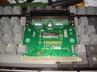
|
|
|
|
|
|
|
Considering the stuff you found out, would it be possible to modify a Master System Converter so it'd incorporate a BIOS? I myself was actually quite disappointed when I played my first Master System game via Converter and was shown the title screen first thing after turning on the console. |
|
|
|
|
|
|
Did you try putting in a game that works with the converter everytime (Hang On/Safari Hunt, Fantasy Zone), powering on, powering off, then inserting the game that doesn't work? I have to do that to get Shinobi to work with my converter. |
|
|
|
|
|
|
|
Wow, thanks TmEE! I was really curious what the adapter looked like.
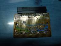
I noticed they are missing a resistor, the one that's present has to be for the Pause button. Since there's no card slot to worry about, I wonder if that freed up an output they could have used to drive Z80 D0. That would explain why there's no second resistor to pull D0 high. They use a Signetics CK2605 which is a cost-reduced version of the PLS153, it's functionally identical but has about half the number of inputs to the OR gates. Not a big deal since the PLS153 was fairly under-utilized in the original PBC. Any chance you'd ever want to trace out the connections between that chip and the SMS cart edge, at least to see if D0 goes to it or not? :D And maybe see if A3 connects to it? (possibility of more ROM data if A3 and higher are connected). mk1995, it would be possible, but you'd have to solder a zillion wires and add a few chips (I think something like a 29EE010 flash and 22V10 GAL at minimum, so you'd need a device programmer that could handle both), and there would be no place to attach them to the PCB so they'd be floating around loose inside the plastic shell. |
|
|
|
|
|
|
I figured that soldering (and tons of it) was going to be a requirement, and I also figured that it mightn't be worth it due to how much work you'd have to put into it, but I'd never thought it'd be this complicated. Fortunately, I wasn't in a mind of actually implementing a BIOS in my Converter, but I'm wondering if somebody else got the idea to try just that (even though the labor/reward ratio might indicate that it isn't really worth it). On a slightly different topic, I wonder what's inside a Master System Converter II. I mean, if you compare the sizes of the two, you'd be wondering how much they actually cut out aside from the card slot. |
|
|
|
|
|
|
Oh that's the thing TmEE posted two pictures of. Despite being smaller and lacking a card slot it is more or less identical to the original Power Base Converter. |
|
|
|
|
|
|
| Oh, whoops. My bad. Should have figured that the circuit board looked a bit off (i.e. couldn't have been for the MSC1), but thanks for the quick elaboration of its contents (which I could probably have found out for myself if I had read the topic more thoroughly... *head meets wall*). | |
|
|
|
|
|
Don't worry, I wasn't sure what it was at first, either. :D All that's left now is to get a peek in the JP Mega Drive's converter and see what they did there. Maybe the same thing as the US one. |
|
|
|
|
|
|
I am interested in building one too. Do you have any reference to the schematic? |
|
|
|
|
|
|
http://dk.toastednet.org/SMS2SMD/sega2sms.png It's messy in there but basically I just took a Sega MD/Gens game I didn't care about (in this case Jurassic Park), desoldered everything from it and cut the whole way across closer to the bottom, then soldered each wire to where it's supposed to go. It took me a few hours (mostly because I would double, triple check, etc) and it works fine. There's various low quality pictures of the finished product too: http://dk.toastednet.org/SMS2SMD/ |
|
|
|
|
|
|
I see, you used the devstar schematic, on his webpage it is stated that he didn't test it, but it then seems it actually works, thanks!
|
|
|
|
|
|
|
|
I tried to my make my own adapter with the Schematic of TmEE and also with the one you posted but it doesn't work, i'm getting only blu screen, white screen etc..
Can you help me to finish this project please 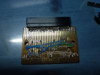
|
|
|
|
|
|
|
| Almost of the wires are blue, there's no way to check what goes where. | |
|
|
|
|
|
|
all the cables goes like this table: (see attached picture)
Black - GND Red - VCC Green - D0 - D7 Blue - A01 - A22 Whiite - SR,CI,WR,OE,CE 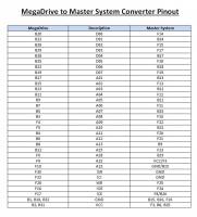
|
|
|
|
|
|
|
|
Did you mistake right / left on the A side?
if you look at the attached pic you see that the data (which in your case should be green) is on the right side of side A (imagine to sit on the left of the page and watch toward the right). In your case it seems to be the opposite 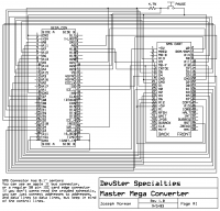
|
|
|
|
|
|
|
|
I think i misunderstood the schematic and the direction of connector.
In the Schemtic Side A is the front side? if yes it's B1 - B32 and if i translate from your schematic B1 =GND, B2 = 5V, B3A8 etc... am i right? Now for the Master System connector it's the opposite (according to the schematic you attached) right? so number 2 of the connector of the master system need to be connected to A4 of the Mega Drive Connector right? can you please post pictures of your adapter you made? |
|
|
|
|
|
|
|
Sorry I didn't make the adapter yet, but this schematic is one everyone seems to use.
Whichever naming conventions you use, the side with GND and VCC is only one (side A in the schematic) From the schematic, I guess A8, A11 and friends should be on the left, and D11 on the right, when you watch the board on that side (A). |
|
|
|
|
|
|
|
I gotta be honest with you I put it together like almost two years ago.
It was a long, tedious process of double and triple checking all the wiring as I did it to make sure it would work. I've also found that if I try to use it in my JVC X'Eye I have to reposition it a few times but it will work. It works perfect first time, every time on my Nomad and Gen Model 1. I don't remember which side was what, I basically just read what he said (connect data to data, addresses to addresses but watch out for the few misc ones laying about). The whole process took me most of the day, like 6 hours or so to build it. I have no high quality pictures as you saw, and it's literally a rats nest in there so any higher res pictures won't help you. It was hard to squeeze it in a really tight space with wires from an IDE cable. EDIT: If you are using this on a Nomad, you have to solder a wire to re-enable the SMS line. You'll have to look on Sega16 for that as I forget which pin it was. |
|
|
|
|
|
|
|
Thank you Maraakate for your help.
I verified my connections 10 times but i didn't any mistakes. It took me only few hours to make the adapter, but i don't understand the way of the connectors. I think i put one of them wrong and because of this it doesn't work, but i can't find any information about this adapter wiring. I need to know what is Side A and B, and how to look to the schematic. From what i saw in internet it's like this. Back A1 --------------------------- A32 | | B1 ---------------------------- B32 Front So side A is Front or Back? I start to go crazy :( |
|
|
|
|
|
|
|
Maybe my page can help a bit more with wiring, etc?
http://www.chrismcovell.com/segahacking/segaadaptor.html "A" seems to be the back of the cartridge. |
|
|
|
|
|
|
| Isn't that not the same thing? | |
|
|
|
|
|
|
Maxim: no the link he gave it's for making an adapter from SMS to Mark III
Ok ok, so Side A is Back and side B is front. Now on the connector of the SMS: 2 -50 is back or front? 1-49 is back or front? |
|
|
|
|
|
|
|
The letters and numbers are usually on the silkscreen.
SMS pins are as here: www.smspower.org/Development/SMSCartridge |
|
|
|
|
|
|
|
Thank Maxim.
Ok so my connector are in the right side and everything is good but it doesn't work and i can't why... |
|
|
|
|
|
|
|
I have to think about it, but I believe the game itself had to be inserted the other way around.
Yes, look at my pictures, see how the game itself is inserted 'backwards'. Try this (obviously with a common game with no battery) and see what happens. |
|
|
|
|
|
|
|
See this table
http://www.hardwarebook.info/Mega_Drive_Cartridge Look at the back. The fourth pin from the left (A4) is address bit A11 you have a (green) data cable connected there as a confirmation of the difference, the page reports B1 B32 Front ========================= A1 A32 Back which is the opposite of your diagram |
|
|
|
|
|
|
|
Thank Kamillebidan but something is strange:
look at the cartridge slot of the MD you will see like this: Back A1 --------------------------- A32 | | B1 ---------------------------- B32 Front if you are looking also at a cartridge PCB of the MD : http://nintendoallstars.w.interia.pl/romlab/ps4cart1.jpg http://nintendoallstars.w.interia.pl/romlab/ps4cart2.jpg you can see that A1 of the PCB is on the right side so the fourth pin from the right is A4 is adress bit A11 and it's blue so no error here or i didn't understand nothing :( Maraakate: i already inserted the game inversed but it doesn't and it should not work also because i did the wiring for having front to front and not to inverse the wa of the game. i have only one game is Sonic 2 i think it's a "simple" game. Thank you for your help all! |
|
|
|
|
|
|
|
dadou,
you are proabably right, I guess the page I found is the cartridge seen from its bottom, and not the slot (seen from the top). That would explain the differences. It still doesn't explain why your adaptor doesn't work though. Are you sure you didn't damage the megadrive during the experiments? do you have an everdrive to test if SMS games still work? Could someone more experienced confirm or deny? |
|
|
|
|
|
|
|
Ok so my connections are good.
i verify also all the trace of the PCB and everything is ok. The Megadrive is working because i can play MD games. No i don't have an everdrive and no other game for SMS. Perhaps the game isn't working but i don't thunk because the game is like new! |
|
|
|
|
|
|
|
Sorry for bumping the topic.
I bought a new game (Super Tennis) 2 weeks ago and tested, i'm getting the same result, black screen. When i'm powering on the console it's like the game trying to start but no sound and no video. someone have an idea? |
|
|
|
|
|
|
| I suspect something similar is also present in the biosless gamegears. Ecco depends on SP pointing to RAM before it works correctly. | |
|
|
|
|
|
| I guess this was the problem with one of the games I was trying to get to work. | |
|
|
|
|
|
| What kind of Genesis Cart can be used to make a MS converter? | |
|
|
|
|
|
| One with al the pins present. They're pretty cheap to buy, though. | |
|
|
|
|
|
| What game do I look for all pins? Do you mean on top of the PCB? | |
|
|
|
|
|
| Will it be a baseball game I can get for a $1 -- What Game works best to make a Converter? | |
|
|
|
|
Homemade Master System Converter
|
|
I'm really want to do this now
What Genesis Cart that as the Pins on top? Is it mainly Sports Games? |
|
|
|
|
|
|
|
Please don't start new threads. I merged your above post back in.
You can tell a cart has all the pins by looking at it. If you have trouble with that then I suspect you'll find the bit where you have to isolate them all, attach a Master System cartridge slot and solder about 50 wires between them even more difficult. It's not a trivial starter project. Are you experienced with this sort of thing? |
|
|
|
|
|
|
| Yeah I know, I wanted someone to answer, I'm going down to my local record store to get some early sports game on the Genesis like Sports Talk Football & Sports Talk 94 | |
|
|
|