|
|
ForumsSega Master System / Mark III / Game GearSG-1000 / SC-3000 / SF-7000 / OMV |
Home - Forums - Games - Scans - Maps - Cheats - Credits Music - Videos - Development - Hacks - Translations - Homebrew |
View topic - Disabling the I/O chip
 |
Goto page 1, 2 Next |
| Author | Message |
|---|---|
|
Disabling the I/O chip
Last edited by Charles MacDonald on Tue Jun 28, 2011 7:20 pm; edited 2 times in total |
|
I figured this was a better place to discuss the region mod.
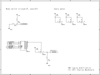
It turns out /KILLGA also disables the I/O chip when writing to ports $00-$3F. You can use this to make a simple region mod that asserts /KILLGA when writing port $3F. This means that port is never initialized, but the power-up settings allow the SMS gamepad to work normally -- remember that the Mark III has no I/O chip and writing to $3F does nothing anyway. Here's a schematic of the region mod circuit. The pull-down resistor R1 is probably not needed as the I/O chip seems to have an internal pull-down on /KILLGA, but I was testing the mod with a part that had weak internal pullups. http://cgfm2.emuviews.com/sms/smsmod1.png The JP_MODE# input should connect to a switch, GND= JP mode, +5V= US mode. I don't have any exotic peripherals to test with it however, but regular games certainly work fine. This should work alongside the FM board. |
|
|
|
|
|
|
|
Hey, this is clever ^^
Do you know if MD region setting works in SMS mode too ? |
|
|
|
|
|
|
|
Sounds like a safer way to get Japanese out of an English system. Nice!
Also TmEE, if you mean will a Mega Drive modded to play Japanese will also play SMS games in Japanese, I can confirm it does. |
|
|
|
|
|
|
| Yes I meant that, and its awesome to know :) | |
|
|
|
|
|
| Very smart! Though it won't work with my FM board because it drives the the KILLGA (named KILLJOY on my diagram) all the time... not such a good idea in retrospect. I'll try this out an publish a fix soon. | |
|
|
|
|
|
Hmm, the circuit only asserts KILLGA during an I/O port write to $3F. Othewise KILLGA isn't asserted (the '125 buffer output is tri-stated) so other devices like the FM board can control it as needed. Shouldn't that be OK? |
|
|
|
|
|
|
| Little confused on how you wire the switch? I am willing to try this out on a spare SMS. Can you update the schematic with the switch in it? | |
|
|
|
|
|
|
Just to clear a few things up, I tried making my own FM board and it works with the Japanese region mod I described earlier, and even with the more troublesome games like Wonder Boy 3 (I also tested Penguin Land and Spellcaster, they sound great).
Here's the schematic and 16V8 fusemap and source: http://cgfm2.emuviews.com/sms/smsfm1.png http://cgfm2.emuviews.com/sms/smsfm1.pld http://cgfm2.emuviews.com/sms/smsfm1.jed This isn't necessarily a good or complete implementation (in particular bit 0 does not mute the FM sound and there's no PSG/FM mixing) but it's what I could whip up to confirm the region mod worked with FM sound. It has independent JP mode and FM enable switches, but you could tie them together to one switch, so one setting is No FM + US mode and the other is FM + JP mode
Sure, no problem. I've updated the schematic in my previous post. Hope it helps. |
|
|
|
|
|
|
|
Are the spare gates wired to ground and will these parts be sufficient for this mod?
http://www.mouser.com/Search/ProductDetail.aspx?R=SN74LS125ANvirtualkey59500000v... http://www.mouser.com/Search/ProductDetail.aspx?R=SN74LS138Nvirtualkey59500000vi... |
|
|
|
|
|
|
Well if you look at the schematic the spare sections of the '125 are tied to +5V but you could wire them to ground as well. Those two parts you linked will do the trick. Good luck. :) |
|
|
|
|
|
|
I'm confused on what pins 6, 8, and 11 go to. Sorry for all the questions, I am new to this. |
|
|
|
|
|
|
| Oh don't worry, those are unused outputs so they don't need to be connected to anything. | |
|
|
|
|
|
Okay, I didn't know if it needed to run to ground to complete a full circuit or something. |
|
|
|
|
|
|
There's an output of a 74HCT device connected to the KILLGA line in the FM board. It's not tri-state, just an ordinary output. Any attempt to drive KILLGA with the FM board connected will result in contention. Also, Maraakate gave me some information that suggests the Pro Action Replay also drives the KILLGA line for some reason... I think a new FM board revision is in order. |
|
|
|
|
|
|
I wish I had a spare PAR to send you your way so you could verify that's the issue. |
|
|
|
|
|
|
Ah, thanks for clearing that up -- I examined the V1.1 schematics on your website and I see what you mean.
Ooh, as in integrating this new region mod into the FM board? :D |
|
|
|
|
|
|
|
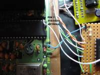
While I was working on 'finalzing' my mod (as seen in the other forum), I stumbled into a surprising behaviour. Basically on my setup, just disconnecting the I/O chip's D7 (315-5216 pin 14) from the BUS's D7 (so Z80 reads HiZ) while boot is enough to fool the system into jap mode on the three carts I've tried WonderBoy I,II and III.
Yes its another fluke perhaps, however this one is safe. Would be cool if someone else could try it out. Of course it means severing one trace underneath the MB. (but i had done this already for the mod) http://picasaweb.google.com/109785470503376823537/SMSFlexiModPart202#5623273048970750498 I'll wait until I get my FM Units and I'll try it with them, at this point I can do any mod I want on a protoboard to the right of the unit http://picasaweb.google.com/109785470503376823537/SMSFlexiModPart202#5623273077792320802 Just add a swtich to open/close the D7 line between Z80 and I/O. |
|
|
|
|
|
|
It's a fluke, the I/O chip input is floating and can take on any value, though most often it goes high. That's what you are seeing with the JP mode working. If you really want to do it this way, add a pull-up resistor to the I/O chip D7. But personally I cannot recommend it. Plus if you leave D7 unconnected the expansion slot can't ever work. I'd really advise doing the second mod (the 74LS138+74LS125 one) where you don't mess with D6, D7, it's much simpler. |
|
|
|
|
|
|
Does it matter whether it floats high or low? As long as it's consistant... |
|
|
|
|
|
|
On a Mark-III reading $DD returns '1' in the upper bits, so it's more accurate to have it high IMO. |
|
|
|
|
|
|
|
I dont think pulling up a shared Data line is wise if its assumed to be sometimes HiZ by a bunch of other chips. I know in theory it shouldnt matter, but practice is often different.
So i'll probably do the original mod, since i need killga alone for FM units (both jap and from viletim) (got all the parts and pins rerouted now). No rush, just fun stuff. |
|
|
|
|
|
|
| Haven't tried this yet. But another question. Do any pins or traces need to be cut for this schematic you've supplied or do you just solder the appropriate data lines and such to the 74 chips? | |
|
|
|
|
|
| I'm going to try to build this circuit with parts I have in my junk box. I don't have any 74574's, but I do have some 74374. It appears to be a tri state d-type flip flop, and I can't tell from the data sheet what the difference between the 574 and 374 is. Would it be a suitable substitute part? | |
|
|
|
|
|
In all honesty it's not a great FM implementation, just what I could whip up with the parts I had. Viletim's board sounds a lot better because he did it the right way with the right parts. And just to be clear you need a device programmer that can program 16V8 chips for the FM mod I posted. The 374 is fine, but take note that the pin assignments on that chip are different compared to a 574. |
|
|
|
|
|
|
|
I was planning on using a 2716 EPROM as a "poor man's GAL" since my eprom programmer can't program GALs.
I might skip the whole thing now because I thought I had an FM PAC MSX cartridge I could pull the ym2413 from, but it turns out it's just a regular PAC cartridge. I could pull it from my MSX2+, but I'd rather not damage it. |
|
|
|
|
|
|
|
I tried the 74ls138 + 74ls125 mod, but it doesn't seem to be working. I hooked up a data probe to take a look, the output going to KILLGA# is high Z, and then pulses high a few seconds after the BIOS runs, and then goes bak to high Z.
Then I tried cutting pin 14 on the I/O chip, and that did the trick. I don't want to lose the use of the expansion port, though... if I was to use a switch or button to break that connection just on bootup and then restore it, would that work? |
|
|
|
|
|
|
Try adding the 4.7K pull-down resistor shown in the schematic. I thought it might not be necessary, but from what you described it is. |
|
|
|
|
|
|
| I'll give that a try... Also I used a 74LS244 as a buffer, but I don't see why that would make a difference. | |
|
|
|
|
|
| The 4.7k resistor did the trick! I've only tested it with Power Strike, but it seems to work. | |
|
|
|
|
|
Great, glad it works! Just to clear up the resistor issue for other readers; I assumed the I/O chip had an internal pull-down resistor on the KILLGA pin to ensure normal operation when that signal isn't being driven. Note that there is no pull-down resistor external to the I/O chip on the SMS schematic. But as it turns out there is no pull-down resistor internal or external to the I/O chip, so you need to add one. What I wonder is, what keeps the KILLGA input from floating high or low when there is no peripheral like the FM board attached? |
|
|
|
|
|
|
I can confirm there is some kind of pull down inside the I/O chip. I measured the pin voltage: 0V with nothing connected, and 0.8V with a 100k resistor to Vcc. |
|
|
|
|
|
|
Very interesting! I wonder why the pin was floating when not driven in blue lander's SMS -- the external pulldown shouldn't have been needed I think. |
|
|
|
|
|
|
|
I think I solved the mystery... I was playing around with Power Strike and noticed it was behaving sporadically - some times it would boot up as Aleste and other times as Power Strike regardless of how I had set the switch, sometimes it wouldn't recognize the cartridge at all. I rechecked the circuit, and realized I had connected ground to the wrong pin on the 74ls244, so ground was floating on that chip.
So I fixed the grounding and double checked everything else, and I'm back to where I started. Killga is low except for right after the BIOS screen disappears and then pulses high, but it still won't switch to Japanese mode. I've tried both with and without the pulldown resistor, doesn't make a difference. I'll triple check the rest of the wiring, but the circuit seems to be behaving as it should... |
|
|
|
|
|
|
| This evening I tried the modification on an original SMS and the SMS 2. It worked as expected. | |
|
|
|
|
|
|
I triple checked the wiring with a multimeter and everything looks okay, no shorts or bad connections. I have one of the older SMS 1's, the one with leaf switches for pause and restart. Does that make a difference?
I also tried manually touching pin 23 to +5, and if I time it just right (about a second after the BIOS music stops), it brings the game up as Aleste. So it works in theory... |
|
|
|
|
|
Last edited by Charles MacDonald on Thu Jul 14, 2011 5:48 pm; edited 1 time in total |
Thank you so much for testing it! I'm glad it worked for you. Maybe if enough people try it, we can tell if this is a viable region mod option or not. |
|
|
|
|
|
|
I'll test Aleste and see what's happening. Do you have other games you can check? I wonder if this particular game does something strange. |
|
|
|
|
|
|
|
I have Psyco Fox and Ghost House handy, but I don't know what (if any) difference there is between SMS and SG-1000 mode on those two.
Just for the heck of it, I tried connecting pin 6 of the 74LS138 to +5 instead of A0. It still didn't work, but with Power Strike I got two pulses in rapid succession rather than the one I got when it was connected to A0. When I put in Psyco Fox or Ghost House, I only got one pulse. |
|
|
|
|
|
|
Yeah if you set pin 6 high the circuit will disable writes to $3E which you don't want. You were seeing the game write to port 3E and 3F with those two pulses. That's what's strange though, if the pulse is there it should be working. Anyway I'd put pin 6 back to Z80 A0. For the LS244, are all unused inputs (1A2, 2A3, etc.) grounded and is the second control input (2G) grounded? There shouldn't be any unconnected inputs on either chip. These same inputs could be tied to +5V if you prefer. Also if you have a 74LS04 you could connect the Y0 output of the LS138 into one of the six gates, and the output directly to KILLGA (getting rid of all pull up/down resistors and the 74LS125). Again, you'd want all other 74LS04 inputs grounded or tied high. I originally had the 74LS125 in there because I wanted to keep the KILLGA line shareable with other peripherals, but it doesn't seem that the official or homebrew FM boards share the line. So regardless of how you do it (LS125 or LS04) don't plug in the FM board/adapter. |
|
|
|
|
|
|
I did leave the inputs on the unused buffer on the 244 floating. I think I'll go ahead and replace the whole chip with a 74hc04 since I have some spares.
Hmm, half the reason I'm doing this is so I could use an FM board with SMS carts... is that possible or do I need to use Mark III games only? |
|
|
|
|
|
|
The FM board will work with games that support it without switching the region to Japanese. There is one exception - Wonder Boy III. It will only play FM sound when it detects a Japanese SMS console. For the next batch of FM boards (will get to it soon!) I'll modify them to drive the JOYKILL line with an open collector output. This way it can be used in conjunction with this region mod. From the sound of it, you must have a faulty '244 or it's still not correctly wired. Instead of the 74LS125 in Charles' diagram I used an PNP transistor connected in the way show below. Best to use what you have though... . ___Vcc . | . | .74ls138 E .pin 15 -----R1-----B Q1 . C . | . R1 = 47k | . R2 = 4.7k R2 . Q1 = any PNP | . | . ---GND |
|
|
|
|
|
|
|
I have some 2N3906 PNP transistors, I'll give your circuit a try. Do I connect Pin15 on the LS138 directly to pin 23 on the 315-6216 as well?
Never mind, I figured it out. It appears to be working! I'll try 6 or 7 more times to make sure it's acting reliably. Thanks for your help. |
|
|
|
|
|
|
| I should have mentioned the output is from the collector of the transistor (the rest is same as Charles' circuit - I didn't feel like rendering it in ASCII). Though it's good to hear that it works! If that 74LS244 was damaged by the wrong ground connection, or never worked properly at all if it was a mystery part from the junk box. | |
|
|
|
|
|
| On a SMS2 which point is KillGA please? Looking at this http://members.iinet.net.au/~stinkyfist/reviletim/smsfm/sms2brd_labeled.png and from Viletims comment I assume pin 1 of 315-5237 chip? | |
|
|
|
|
|
| Ok tried this in a SMS2 and I can't get it to work. Am I supposed to lift pin 1 on the 315-5237 chip? I have double checked and triple checked my wiring and it is all good. | |
|
|
|
|
|
|
You lift no pins, but solder directly on them.
There are pinouts available of various chips here. You can find pinouts of SMS2 chips from forum search, there should be 2 big threads. |
|
|
|
|
|
|
| Got confirmation from Tim it it is pin 1 (he labelled as Joykill). For today I am over this one (finished FM board install and S-video). I will re-visit it, if again it doesn't work I will do up a CAD drawing of how I wired it to see if others can see what I have missed. | |
|
|
|
|
|
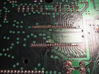
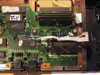
Dagnab it! Still doesn't work. I made the little vero board bigger and laid everything out logically. Could someone please look at these pics and tell me where I am going wrong?
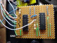
Image 1 shows my little board with the 74LS138, 74LS125 and 2x 4.7k Ohm resistors. +5v rail runs along the top, GND along the bottom. 74LS138 pin 1 goes to the switch pin 2 goes to Z80A7 (pin 37 on Z80) pin 3 goes to Z80A6 (pin 36 on Z80) pin 4 goes to Z80WR (pin 22 on Z80) pin 5 goes to Z80IORQ (pin 20 on Z80) pin 6 goes to Z80A0 (pin 30 on Z80) pin 7 N/C pin 8 GND pin 9 to pn 14 N/C pin 15 goes to pin 1 74LS125 pin 16 +5v 74LS125 pin 1 goes to pin 15 74LS138 pin 2 goes to +5v pin 3 goes to 4.7k ohm (then to GND) as well as pin 1 315-5237 pin 4 & pin 5 are joined then onto GND pin 6 N/C pin 7 GND pin 8 N/C pin 9 & pin 10 are joined onto GND pin 11 N/C pin 12 & pin 13 are joined onto GND pin 14 +5v image 2 shows the points on the board for +5v, GND and pin 1 (315-5237) 
image 3 shows the Z80 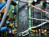
IORQ pin 20 WR pin 22 A0 pin 30 A6 pin 36 A7 pin 37 Any help would be just jim-dandy Cheers Pete [attachment fairy was here] |
|
|
|
|
|
|
|
omp,
Disconnect your circuit board from the master system. Test 1: Check to see the I/O disable line works. With the SMS turned on and playing a game, connect the Joykill line to +5V (ideally through a 1k resistor to prevent 'accidents'). The gamepad should stop responding wiile this line is high. Test 2: Check to see if your modification circuit is working correctly. Connect A7, A6, /WR, and /IORQ to ground. Connect A0 to +5V. Measure the output with a voltmeter. When the switch is open the output will be around zero volts, when closed the output will be around 5V. Note that this is a test for the modification board in isolation, ideally you should power it from an 5V dc power supply and leave the SMS out of the equation altogether. Test 3: Check that your solder points to the SMS board are correct. Go to Dev section of SMS Power and fetch the cartridge slot pinout diagram. Use a multimeter on the continuity setting to check that the solder points have continuity to the equivalent pins on the cartridge slot. Note the Joykill aka /KillGA signal is known as JyDs on this diagram. BTW, Please scale your images if you are going to embed them in a post. |
|
|
|
|
|
|
|
Thanks Tim for the reply
Done the tests 1/Pass tested on Alex Kidd, when 5v (through 1k resistor) is applied, he jumos then ducks. control pad stops working 2/Not sure on this one. took board out and tested away from console. Switch open 0Vdc, switch closed 3.8Vdc. Would 3.8 be to low? 3/Pass, all connections were sound before removing board. Sorry about size of pics. But hang on, if this mod applies 5vdc to joykill and disables the controller, how does it go into JPN mode and be able to play a game? |
|
|
|
 |
Goto page 1, 2 Next |

