|
|
ForumsSega Master System / Mark III / Game GearSG-1000 / SC-3000 / SF-7000 / OMV |
Home - Forums - Games - Scans - Maps - Cheats - Credits Music - Videos - Development - Hacks - Translations - Homebrew |
View topic - CPU replacement
 |
| Author | Message |
|---|---|
|
CPU replacement
|
|
I just bought a couple of 20Mhz Z80, yes it exist, in DIP package, pin to pin compatible with the old version :) and before I make an electronic slaughter I have some questions:
1) Is someone know the maximum speed work and access time of the other SMS chips (memory, VDP)? 2) I never open a SMS2, the Z80 it is DIP or CMS package, on socket? Since most game synchronise with the VDP, actual speed gain is mainly for time-eating CPU routines, but I think it can be interresting to try. I think I can start with the 10,7Mhz SMS crystal. |
|
|
|
|
|
|
|
The Z80 is your regular DIP black-lump-with-legs thingumabob.
Note, however, that: 1. The 10.6MHz crystal controls everything - the PSG, the RF modulator, presumably also the VDP. You might want to try disconnecting the Z80 from the clock and suppyling a new clock just to that. 2. The CPU can't access the VDP too fast during the active display or there will be bus contention resulting in on-screen corruption. Most games use cycle-counting to time VDP accesses, so an overclocked CPU will cause problems. However, in my experiments, the timing guidelines in the Sega developers' documents are about 25% more than necessary so you might get a little speed-up. |
|
|
|
|
|
|
|
Thanks for the info,
some time ago I found an interresting schematic for MSX computer, therefore Z80 system, wich is able to swith automaticly between original clock and your own signal. It's scan Z80 control bus (IRQ, IO, etc) and switch to original clock ONLY if it need to access external chip, since all the process is numeric there is no parasite and very High stability. I would rather use the original 10,6Mhz Crystal in order to increase system stability, it's for avoid "dephasing" signal between Z80 and other chip. But since a lot of guy use external oscillator, I suppose it's not so grave. Just a last precision, it's not overclocking, since the 20 Mhz Z80 can indeed handle High Speed clock. According to my original Thomson Z80 Datasheet (in France it's the Zilog clone maker), the Z80 4Mhz can accept up to 5,5Mhz without notable overheat, BUT such speed make it unstable. It's the reason I want use high speed Z80, so I can be sure Z80 is not the problem. http://members.chello.nl/h.otten/superturbo/circuit.gif |
|
|
|
|
|
|
|
I'm really sorry, but you can forgot all I say before, my vendor scrambled his reference ( and my patronnage by the way), I am the happy owner of two Z80 **PIO** not CPU, it was too good to be true :( well if someone as an old arcade PCB to repair...
However,I have always a 6Mhz version, it's a good start... |
|
|
|
|
|
SMS overclocked
|
|
I 'overclocked' my SMS (underclocked it too!) a year or so ago by supplying an external clock signal to the CPU, the original CPU. Basically the most carts can be accessed by a CPU at 8MHz (given the Z80 memory cycle and 250nS ROMs), the internal DRAM is OK for 12MHz from memory, and the PSG and IO can probably latch at high speed, but the real bottle neck is the VDP. Graphic corruptions occur when the Z80 speed is increased by the slightest bit. An elaborate solution to detect IO accesses to the VDP and signal the CPU wait line to insert wait states in the access and also between consecutive VDP accesses. But who's going to do that.
Increasing the System clock speed will affect everything, including frame rate. |
|
|
|
|
|
|
Since the superturbo schematics is fully configurable, maybe we can work with a 6Mhz clock or better, and revert to original clock ONLY on VDP access. The guy who create this system is really clever. |
|
|
|
|
|
|
|
The problem is that you need to slow down between VDP accesses. This old post shows that, on my SMS2, you need a minimum 26 cycle delay between accesses during the active display, with the most conservative documentation recommending 29 cycles during active display and 16 cycles during inactive display. This works out at about 8us so you'd need it to clock the Z80 to the standard speed for that long immediately after each VDP access (assuming an instant response). I don't know if the "superturbo" can do that.
I don't remember Charles finding different results when he tested it on other hardware but I don't remember very clearly. |
|
|
|
|
|
CPU wait
|
|
Maxim is right. The 8uS interval comes from the VDP allocating 1 in every 16 VRAM accesses to the CPU interface during active-scan period. It's something like 16 x 372nS = 5.95uS in addition to the 2uS interval usually require between CPU-VRAM accesses. Write within that period and you overwrite pending VRAM data before the VDP and fetch it and write it to VRAM, causing graphics corruption.
I don't like the idea of a variable clock. I think a one-shot timer that is triggered when VDP is accessed that will assert the Z80 wait pin if it tries to access the VDP within the timer period and make it wait until the timer period is over is a better solution, if you really wanted to do it. |
|
|
|
|
|
|
|
Maybe it's possible to tweak the timer length, maybe it doesn't really matter if it's a bit long. The latest figure I have: 23 cycles on a PAL SMS (where I tested) makes 7.33us. I'd be interested to see how this works.
Another thing I noticed in old forum posts, browsing for various stuff and reading old threads: some games can't be overclocked reliably. Changing (or adding) the IPERIOD line in meka.nam will emulate CPU-only overclocking and some games (Road Rash, at least) show errors, presumably because of timing-sensitive code. Also, you'd expect samples to play too fast on an overclocked CPU because they use cycle-counting. |
|
|
|
|
|
|
Take look at the schematic, you can modify the "slow" delay by tweaking the R5/C5 circuit, after all MSX and SMS VDP are similar. the full superturbo site is: http://members.chello.nl/h.otten/superturbo/supturbo.htm the first part can be used to apply Asynchronous idea too.
Of course, such system must contain a "force slow switch" ;) Just a last thought, maybe I don't clearly understand your last posts, but is VDP access critical during video memory access only or during all VDP access? |
|
|
|
|
|
wait state controller design, and overclocking
|
|
Making the delay / interval time adjustable isn't a problem. On a one-shot timer solution where the timing is cntrolled by a RC combination, making the R adjustable will allow the interval to be varied.
Of course if I was going to build such a thing (which I most likely will not be building, so feel free to use the idea) then it would be logic not RC based, and actually count the number of clock CPU cycles since a VDP access. The minimum number of cycles between VDP access can be set using DIP switches or a latch. The whole design could be implemented on a microcontroller or using common 74HC logic, like a bin counter with a 4-bit magnitude comparator, etc... The bin counter and comparator can also be used to divide a faster clock from the SMS system clock, for some sweet configurable CPU overclocking. Observe: Divide by Speed (MHz) 1 53.2034 (PAL SMS sys clock) 2 26.6017 3 17.7344 4 13.3008 5 10.6406 6 8.86723 7 7.60048 8 6.65042 9 5.91148 10 5.3203 11 4.8366 12 4.4336 13 4.0925 14 3.8002 (overclocked) 15 3.5468 (std PAL SMS speed) |
|
|
|
|
|
|
Sorry to bump an old post, but did anybody ever finish adopting this design for SMS? It's a fascinating circuit, and was tricky to track down since the above link is now dead. Fortunately, it was backed up by MSX fans here: https://hansotten.file-hunter.com/do-it-yourself/clock-upgrades/#circuit I also uploaded the schematic for preservation sake here. I could build the circuit, and design a PCB for it but I don't understand enough about the SMS architecture to know which inputs should be used to signal the circuit back to a stock clock. Anyone want to help point me in the right direction? I'm assuming memory request would be a good place to start The oscillator inputs could be improved in various ways with modern circuitry as well. It would be so cool to max out a 6MHz overclock without graphical corruption. 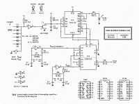
|
|
|
|
|
|
|
|
It’s all to do with accesses to things which require time to respond, and the slowest are all on the IO bus. The only question is how long to go in “slow mode” for - I guess the slowest scenario is sample playback. This uses cycle counting but also sometimes very low sampling rates - so if we have a 4kHz sample then you need to go slow for 900us per port access.
One other thing I know includes cycle counting (of sorts) - 50/60Hz detection counts cycles for a frame. A turbo CPU could well overflow the counter and give you somewhat a somewhat arbitrary result. So a hardware switch would be needed for those cases. I’m not sure what speed you can go for RAM and ROM accesses, plus mapper changes. Presumably you can’t go slow that for all memory accesses because then opcode fetches would make you slow all the time? |
|
|
|
|
|
CPU replacement
|
|
Going by the circuit you would disconnect the CLK trace from the Z80's CLK pin and connect the "Clock Out" line from the circuit to it instead. Then connect the IORQ line from the Z80 to the circuit where it says "IORQ".
The Super Turbo circuit looks like it switches out a fast clock speed for a slow clock speed for IO read or write cycles. This will help if the CPU is clocked faster than the default 3.55/3.58MHz to the point that the IO device can't work with the CPU. However it won't prevent graphics glitches that occur when the CPU writes to the VDP faster than the interval needed during active display. That would need some sort of WAIT state generator. Going by the TMS9918 and Z80 timing diagrams, the length of the WR strobe required by the VDP (200nS) limits the max CPU speed to around 12MHz. The time the VDP requires data on the data bus to be stable after the WR strobe is released (30nS) limits the CPU speed to around the 6MHz mark. Trial and error will determine the actual limits though. I overclocked the CPU in my SMS to 4.6MHz years ago. I only tested it with a couple of games though, the main game being Power Strike. At 4.6MHz there were a couple of graphical glitches on the title screen, however game play was fine and it even got rid of the frame-skip when the action got heavy. |
|
|
|
|
|
|
| Could you use the vdp interrupt pin to tell you when the screen is active and either slow the clock, or insert waits, for any vdp writes during active screen? Obviously software that uses cpu cycle counts is still going to be a problem i guess tho. | |
|
|
|
|
CPU replacement
|
|
Yeah that's what I was thinking.
Assuming most games use the default 192-line display, and using the 10.7MHz VDP clock which is double the pixel clock as a counter that resets each interrupt, wait states wouldn't need to be generated for the first 70x342=23,940 pixels after an interrupt for NTSC or 120x342=41,040 pixels for PAL. After that point, and up to the next interrupt when the counter resets, if a write to the VDP data port occurs within 32 pixels from the last write to the VDP data port, then wait states can be generated to stretch the interval out to 32 pixels. Seems like a lot of effort though. And it might not even work in practice. :) |
|
|
|
|
|
|
|
Hey, good to see ya around wasup.
Well this is exactly what the above circuit does. It swaps the regular clock for a higher one, and lets you use a data signal to determine the switch. Obviously an RC filter can be added to adjust the timing as well. Using the VDP interrupt is a good idea. What's the name of that pin exactly? The circuit is a bit of a pain to build, but not as hard as others I've done. I could design a circuit board for it if there was interest. Or when I get free time. I just needed to know a couple of data lines to feed it and test. And the VDP interrupt sounds like a good idea. I can design a simple RC to adjust in real time without doing a bunch of crazy calculations trying to figure out at what state the CPU will be bothered (i.e. During which cycle count or how many pixels, writes, etc). I can just test it in a real-world environment and see what happens. I'm just thinking that this looks highly possible. And it would be cool to have a 6Mhz SMS :) From my testing, even a 4Mhz OC will add graphical glitches in a number of games. So a circuit like this could help a lot. Thanks for the input and Technical know how everyone! |
|
|
|
|
|
|
|
I would use the vdp clock (but divide by 2) to clock the z80. Itll work out close to 6mhz. The interrupt pin is labled int on the circuit diagram in the service manual.. sorry a bit tricky to look at that on my phone and give a pin number.
You will likely want to AND the int pin along with vdp writes to give you a triger. |
|
|
|
|
|
|
That makes a lot of sense. I feel like I'm finally getting a firmer grasp on this circuit. So between the VDP and Z80 theres !WR but theres also an interrupt (!IORQ) in addition to the main !INT signal. Should I consider using that as well or just the !WR and !INT? Doing an AND is a good idea. I have a bunch of 74 logic chips in the parts bin I can use. I also totally agree that it makes perfect sense to do 1/2 the VDP clock. Sorry if my understanding of interrupts is not so great, my programming knowledge still has a ways to go. For the circuit, I feel like I understand it pretty well as it's just using flip flops and inverters mostly. The RC of R5 and C5 work together to slowly bring the state to OC, i.e. if theres a lot of interrupts happening quickly then it wont do a bunch of fast flipping between OC and stock, which is a good thing. |
|
|
|
|
|
|
|
I would use /IOREQ along with write.
I ordered some 20Mhz Z80's off aliexpress, which have arrived. If i get some time soon ill have a look at trying this too. 
|
|
|
|
|
|
|
| great!! :D are you going to design a PCB? | |
|
|
|
|
|
|
|
|
|
|
Thats an interesting video! These are totally sanded down and remarked. You can see it on the ejector marks.. or lack of. Fail! Ill chuck one on a sms2 when i get a chance and see if they actually work. If they do work i bet they are 4mhz rebadged as 20mhz. I did also buy some new ones from rs components which will be real.. i got some 6, 8 and 10mhz to have a play with. |
|
|
|
|
|
|
Did you ever get anywhere with this? I'd love to have a cpu overclock detached from vdp issues |
|
|
|
|
|
|
|
Hello, I made this a while ago, It's for SMS2 tho.
https://www.smspower.org/forums/18057-RGBSMS2GlitchFreeOverclocking |
|
|
|
|