|
|
ForumsSega Master System / Mark III / Game GearSG-1000 / SC-3000 / SF-7000 / OMV |
Home - Forums - Games - Scans - Maps - Cheats - Credits Music - Videos - Development - Hacks - Translations - Homebrew |
View topic - Power Base VA3 PCB layout
 |
| Author | Message |
|---|---|
|
Power Base VA3 PCB layout
|
|
Hi at all,
i'm in searching for the pcb layout, and SM for the VA3 power base. I need to service some bad traces around the Z80, and the bios in my one. The service manual for the VA3, on the net is impossible to find. Thanks at all. Toshio |
|
|
|
|
|
|
|
Or anyone have a photo, of the Z80, Rom, Ram
without the IC, to see the pcb traces under those? 
I ask for this, i don't have a good desoldering tools to remove this IC's. And i want to repair the pcb from the other side of the board. Thanks again, Toshio. 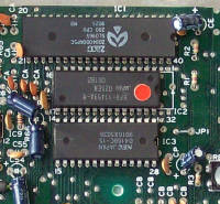
|
|
|
|
|
|
|
|
Master System 1 service manual: https://www.smspower.org/Development/SegaMasterSystemServiceManual
Master System 2 service manual: https://www.smspower.org/Development/SegaMasterSystemServiceManual I realize it may not be the exact same revision but these should help. |
|
|
|
|
|
|
|
Thanks maraakate.
it's help at some point, but i have buyed a desoldering iron, i wanna to go deep, to see all pcb trace under those 3 ic. When i removed the ic i posted the photo's. Thanks. Toshio |
|
|
|
|
|
|
| Just follow the schematic. They're practically the same. You risk damaging the board with desoldering that many pins and the board is pushing 35 years old. | |
|
|
|
|
Power Base VA3 PCB layout
|
I second this. The traces are very fragile and easily damaged. The ROM and RAM chips have very similar pinout with only a couple of lines different between the two, e.g. /WR, CE. So most of the traces between the ROM and RAM (address, data) run in parallel between the 2 chips. |
|
|
|
|
|
|
Don't worry is a good desoldering station. Thanks, Toshio |
|
|
|
|
|
|
Not to be rude, but if you don't have desoldering equipment already and do not know how to figure this out by following the schematic then you really shouldn't be attempting this. Desoldering this stuff is a lot harder than you think. It's not just removing a capacitor. Get a logic probe and use your ohm meter to find out if there is a bad trace or if one of the chips is faulty via the logic probe. Get a logic probe and use your ohm meter to follow the schematic from one pin to wherever it leads. If you need help on which specific areas to focus on then please ask. Blind replacement of components is not diagnostics. |
|
|
|
|
|
|
|
Maraakate, ok.
Teach me how is connected the path of bios, ram, and z80 in this schematic portion. It's very difficult to me to understand: 
Thanks again, Toshio 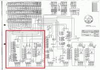
|
|
|
|
|
|
|
|
For example pin 30 of IC1 (Z80) is connected to pin 10 of IC2 (ROM) is connected to pin 10 of IC3 (RAM) because they are all labelled with the net "A0". Same for the other labels. If the labels are different then the pins are not connected.
Labels outside of the box are more important than those inside, so for example pin 20 of IC2 is the net #EXM2 (when I write # it's when there is a line over the name on the schematic) and *not* a net called #OE. If you are having problem reading the schematic, because the photocopy is a bit faded, you can always look at the datasheets to see the pinouts. This will also help you understand the pin numbering, which runs anti-clockwise from the top left pin to the top right pin. For example, random Z80 pinout from internet uPD4168 (IC3) datasheet with pinout on page 1 |
|
|
|
|
|
|
|
Thanks Will,
i have a short to pin1 (vpp) of IC2, pin 27 of the IC3 (WR) and the pin22 (WR) of the Z80 all together. It's normal? Thanks, Toshio |
|
|
|
|
|
|
|
That pin 27 of IC3 and pin 22 of IC1 are connected is expected since they are both the #WR net.
However if that net appears to have a hard short to Vcc then that is potentially a bad thing. Is it definitely a hard short, i.e. a continuous resistance very close to 0 ohms, measured with an ohmmeter and the power off? EDIT: Vcc is very widespread over the PCB, so you should be able to confirm a short by measuring for continuity between pin 22 of IC1 and any of the other various points that provide Vcc, e.g. 26 of IC3, 11 of IC1, 32 of IC4 etc. You never said what the fault with your system was — is it completely non-functional? |
|
|
|
|
|
|
|
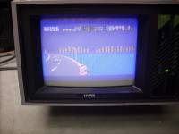
I have a full power on, led on, but black screen pratically freeze.
And i don't understand the pin 1 of IC2 (vpp) are connected to the pin 22 of the Z80 and the pin 27 of IC3. And another thing, the pin1 of IC2 are not connected to the vcc rail. Sorry for misunderstand. Any dead short to ground on the Vcc rail in fact is in power on. I spot other bad interrupt traces on the pcb under the z80. I need to repair it. But now i understand to read the schematic, but is a very real bad photocopy. Toshio |
|
|
|
|
|
|
|
The M4 revision are, very identical to the VA3.
Like said Will the pin 22 of the Z80, the pin27 of IC3, are connected together, but the pin 1 of IC2 are connect together to those. The M4 revision is very like the VA3: 
Toshio 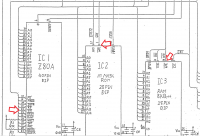
|
|
|
|
|
|
|
| Yep okay that makes more sense then. Good luck figuring out the problem. As others have said, go slowly and carefully. Repairs on traces are not easy. | |
|
|
|
|
|
|
Yes, in what you just showed the "short" i.e. 0 ohm resistance means those lines are connected.
IC1 pin 22 should have 0 ohms to IC2 pin 1 and pin 27 of IC3, which is what you have so that line is good. If you find something that is supposed to be connected and it reads infinity that means there is a severed trace somewhere. A unit that turns on with a black screen with no audio and the unit has not been modified and looks like a clean board that has been stored well tends to mean one of the ICs is bad. I can't answer specifically which one as I haven't repaired one of those myself. But, I believe (and someone correct me if I am wrong) that it's usually the CPU/Z80 or RAM. |
|
|
|
|
|
Last edited by Toshio on Wed Sep 06, 2023 11:02 pm; edited 1 time in total |
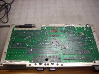
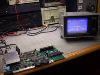
After repair many traces, now is fully working:


The trace repair, i'm sorry for not perfect work on tht: 

Now still waiting the Japanese bios. Thanks at all, Toshio 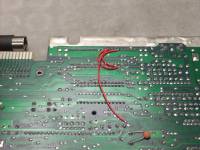
|
|
|
|
|
|
|
|
Very nice! Congrats!
Which lines needed repaired? |
|
|
|
|
|
|
|
Great work, what a result!
That repair job looks very neat to me. I'm also interested in what traces were faulty. That board looks like it's in exceptionally good condition. Have you recapped it? If the old capacitors had leaked sometimes the residue can cause faults. |
|
|
|
|
|
|
As in schematic:

No never reccaped as a factory mint. The capacitor are not leak, near the IC's. Thanks. Toshio 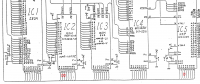
|
|
|
|
|