|
|
ForumsSega Master System / Mark III / Game GearSG-1000 / SC-3000 / SF-7000 / OMV |
Home - Forums - Games - Scans - Maps - Cheats - Credits Music - Videos - Development - Hacks - Translations - Homebrew |
View topic - My first SMS simple platform game test
 |
Goto page Previous 1, 2 |
| Author | Message |
|---|---|
|
|
|
I would like to change the existing code (WLA-Z80) for SMS to run on GG. I don't know if it's enough:
1. Limit (when creating) the displayed graphics 256x192 to 160x144 (top / bottom - 3 rows of tiles invisible, left / right - invisible 6 columns on each side) 2. Changing the defined color palette from 1-byte to 2-byte (SMS 32 bytes, GG 64 bytes). 3. And optionally, the use of an additional pad reading port to use the START button. Please correct me if I think something wrong. And if any changes to VDP initialization are required, any additional things like info e.g. some GG HEADER etc. |
|
|
|
|
|
|
|
Actually GG screen is exactly the same as SMS.
nothing to change, the visible part will only be 160x144 on the center (can be elsewhere but its more complicated) if you use frame interrupt (at 192) for your VBL routine, you can always use it, but if you want to maximise performances you must do it manually : detect line 168 => screen off. Then wait line 24 => screen on (or as soon as your vbl things are done, easier, but you must be sure of your code) Lines between 168 and 192 are always active even if outside the GG screen (as its derivated from the SMS) so be carefull with VRAM writes ;) only real things to change : - palette (16bits) instead of 8bits - pause no longer works, $66 is for NMI/G2G - crt0 must be slightly updated (accordingly to the GG official doc) ; wait vdp to be ready (spec GG, can be /reset at start)
init_wait: in a, (Port_VCounter) cp #0xB0 jr nz, init_wait A little note about VRAM writes, as it exists GG with 2 Asics (VA0/first models) and 1 Asic (>VA0). You must wait at least 27 cycles between VRAM writes to be good for every GG (in active part of the screen, to update a background tilemap for example). Less than 27 cycles on 2 asics will produce glitches. There is a thread in the forum with tests from Sverx and other members about this problem. https://www.smspower.org/forums/15852-PhantasyStarOnEverdriveGlitches?start=50#1... |
|
|
|
|
|
|
Thanks for the info. Yes. I know that, I meant these "invisible" parts of the screen. I did my first test demo on Game Gear: https://dl.dropboxusercontent.com/s/qqrlu97vgeyo2xy/platform_demo_gamegear.gg It works on emulators, but I don't know about real hardware. I used vdp wait code as well. Maybe I remember something wrong, but once I read about some additional code for SGG, the lack of which meant that on some models it may not work (or I remember something wrong ...). |
|
|
|
|
|
|
basically it's just that 26 CPU cycles between writes to VRAM is always safe on *any* SMS but it turned out not to be safe on *every* GG. 27 CPU cycles should be safe on all of them. |
|
|
|
|
|
|
| I mean a certain piece of the "TMSS" code for GG - it is possible that I remembered something incorrectly because I thought that I read about it somewhere before but I don't remember where. | |
|
|
|
|
|
You probably mean this, then. Yes, GG BIOS (present on some models) checks if there's a specific string written at some specific location. |
|
|
|
|
|
|
| However that check is a subset of what you need for SMS anyway. | |
|
|
|
|
|
| To tell you the truth, I did not set it up in my SMS code - will it stop running on real hardware? | |
|
|
|
|
|
|
Export (that is European/American) SMS checks the SEGA header, if it's not there, or if the checksum is not correct, it won't start the game.
Game Gear equipped with a BIOS (only some models) will check the SEGA header too, won't start the game if it's not found. |
|
|
|
|
|
|
| Just out of curiosity - copying the 7FF0-7FFF range from "other" roms of the same size and type (JUE / W) will work correctly? | |
|
|
|
|
|
|
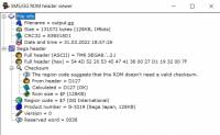
No, the checksum needs to be correct. WLA DX supports computing this directly, else you can use https://www.smspower.org/maxim/Software/HeaderReader to check it.
To boot on a Game Gear with a pre-game splash screen you need: - "TMR SEGA" at $7ff0 To boot on a Master System with BIOS checks (i.e. US and European systems) you need: - "TMR SEGA" at $7ff0 - A valid region code in the high 4 bits at $7fff - 0x4 is good - A valid checksum range in the low 4 bits at $7fff - 0xc means 32KB - A valid checksum value at $7ffa-b. This is the word-wise sum of all the bytes in the checksum range, except for the 16 bytes header area from 0x7ff0-f. |
|
|
|
|
|
|
|
I checked copying 16-bytes from another ROM manually to $7FF0, and then performed checksum repair using "Master System Checksum Fixer" - can this method work? It seems to work, but of course I can be wrong.
https://www.smspower.org/forums/16629-MasterSystemChecksumFixer In the attachment there are two ROM SMS and GG files with a header added this way. 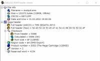
|
|
|
|
|
|
|
| far easier : use the .SMSTAG directive in WLADx ^^ | |
|
|
|
|
|
|
It works too, of course. Out of curiosity, I am interested in whether this "manual" method works.
Another question: What do I have to pay attention to when rewriting the SG-1000 code to ColecoVision? To my eye, the only differences I noticed are the ROM starts at $ 8000 instead of $ 0000, WRAM starts at $ 6000 instead of $ C000 and the registers / ports themselves are the same. |
|
|
|
|
|
|
As Maxim said. The simpliest is a basic addition from 0 to 7FEF and set it as a Western 32Kb rom (faster boot). Just keep in mind that checksum is little endian and you're good. |
|
|
|
|
|
|
|
I have a problem with creating a subroutine table, I don't know how to do it correctly in WLA-Z80:
LD HL,LEV_TBL LD D,0 LD A,(LEV_Index) RL A LD E,A ADD HL,DE JP (HL) LEV_TBL: .DW LoadLEV000,LoadLEV001,LoadLEV002,LoadLEV003,LoadLEV004,LoadLEV005,LoadLEV006,LoadLEV007 .DW LoadLEV008,LoadLEV009,LoadLEV010,LoadLEV011,LoadLEV012,LoadLEV013,LoadLEV014,LoadLEV015 .DW LoadLEV016,LoadLEV017,LoadLEV018,LoadLEV019,LoadLEV020,LoadLEV021,LoadLEV022,LoadLEV023 .DW LoadLEV024,LoadLEV025,LoadLEV026,LoadLEV027,LoadLEV028,LoadLEV029,LoadLEV030,LoadLEV031 .DW LoadLEV032,LoadLEV033,LoadLEV034,LoadLEV035,LoadLEV036,LoadLEV037,LoadLEV038,LoadLEV039 .DW LoadLEV040,LoadLEV041,LoadLEV042,LoadLEV043,LoadLEV044,LoadLEV045,LoadLEV046,LoadLEV047 .DW LoadLEV048,LoadLEV049,LoadLEV050,LoadLEV051,LoadLEV052,LoadLEV053,LoadLEV054,LoadLEV055 .DW LoadLEV056,LoadLEV057,LoadLEV058,LoadLEV059,LoadLEV060,LoadLEV061,LoadLEV062,LoadLEV063 also does not work: ; .DW (LoadLEV000),(LoadLEV001),(LoadLEV002),(LoadLEV003),(LoadLEV004),(LoadLEV005),(LoadLEV006),(LoadLEV007) ; .DW (LoadLEV008),(LoadLEV009),(LoadLEV010),(LoadLEV011),(LoadLEV012),(LoadLEV013),(LoadLEV014),(LoadLEV015) ; .DW (LoadLEV016),(LoadLEV017),(LoadLEV018),(LoadLEV019),(LoadLEV020),(LoadLEV021),(LoadLEV022),(LoadLEV023) ; .DW (LoadLEV024),(LoadLEV025),(LoadLEV026),(LoadLEV027),(LoadLEV028),(LoadLEV029),(LoadLEV030),(LoadLEV031) ; .DW (LoadLEV032),(LoadLEV033),(LoadLEV034),(LoadLEV035),(LoadLEV036),(LoadLEV037),(LoadLEV038),(LoadLEV039) ; .DW (LoadLEV040),(LoadLEV041),(LoadLEV042),(LoadLEV043),(LoadLEV044),(LoadLEV045),(LoadLEV046),(LoadLEV047) ; .DW (LoadLEV048),(LoadLEV049),(LoadLEV050),(LoadLEV051),(LoadLEV052),(LoadLEV053),(LoadLEV054),(LoadLEV055) ; .DW (LoadLEV056),(LoadLEV057),(LoadLEV058),(LoadLEV059),(LoadLEV060),(LoadLEV061),(LoadLEV062),(LoadLEV063) The HL address does not correctly point to the address of the LoadLEVxxx function, it only points to the address of the Table itself in ROM. I don't know how to make such a table in WLA. LoadLEV000: ; code RET LoadLEV001: ; code RET (...) LoadLEV127: ; code RET |
|
|
|
|
|
|
|
try with sla a or add a instead of your rl a
easy to check with a step-by-step debugger if your LEV_TBL table is aligned (on a $xx00 address) you can also only change the L part of HL (faster) |
|
|
|
|
|
|
|
note that
JP (HL)
is actually loading the value of HL into the program counter, so you should point to your table like you're doing, then load two bytes from there, put the value in HL and then jump LD HL,LEV_TBL
LD D,0 LD A,(LEV_Index) RL A LD E,A ADD HL,DE ld e,(hl) inc hl ld d,(hl) ex de,hl JP (HL) |
|
|
|
|
|
|
|
I use variations of the below code (the example is a jump table containing game states, but it should be similar to your case):
main_loop:
ld a,(game_state) ; Get current game state - it will serve as JT offset. add a,a ; Double it up because jump table is word-sized. ld h,0 ; Set up HL as the jump table offset. ld l,a ld de,game_states ; Point to JT base address add hl,de ; Apply offset to base address. ld a,(hl) ; Get LSB from table. inc hl ; Increment pointer. ld h,(hl) ; Get MSB from table. ld l,a ; HL now contains the address of the state handler. jp (hl) ; Jump to this handler - note, not call! ; --------------------------------------------------------------------------- game_states: .dw initialize_metasprite_demo, run_metasprite_demo __: |
|
|
|
|
|
|
|
This is code rewritten from my old 6502 code, so I don't want to change everything, just leave a similar working principle.
Works properly now. (...) SLA A LD E,A ADD HL,DE LD E,(HL) INC HL LD D,(HL) EX DE,HL JP (HL) I guess Using the SLA on the Index (Word Table), I will have problems if the number of levels is 000-255 (it will limit me to 000-127) LD A,LEV_TBL_HIGH LD H,A LD A,LEV_TBL_LOW LD L,A LEV_TBL_HIGH: .DB HIBYTE(LoadLEV000),HIBYTE(LoadLEV001),HIBYTE(LoadLEV002),HIBYTE(LoadLEV003),HIBYTE(LoadLEV004),HIBYTE(LoadLEV005),HIBYTE(LoadLEV006),HIBYTE(LoadLEV007) .DB HIBYTE(LoadLEV008),HIBYTE(LoadLEV009),HIBYTE(LoadLEV010),HIBYTE(LoadLEV011),HIBYTE(LoadLEV012),HIBYTE(LoadLEV013),HIBYTE(LoadLEV014),HIBYTE(LoadLEV015) .DB HIBYTE(LoadLEV016),HIBYTE(LoadLEV017),HIBYTE(LoadLEV018),HIBYTE(LoadLEV019),HIBYTE(LoadLEV020),HIBYTE(LoadLEV021),HIBYTE(LoadLEV022),HIBYTE(LoadLEV023) .DB HIBYTE(LoadLEV024),HIBYTE(LoadLEV025),HIBYTE(LoadLEV026),HIBYTE(LoadLEV027),HIBYTE(LoadLEV028),HIBYTE(LoadLEV029),HIBYTE(LoadLEV030),HIBYTE(LoadLEV031) .DB HIBYTE(LoadLEV032),HIBYTE(LoadLEV033),HIBYTE(LoadLEV034),HIBYTE(LoadLEV035),HIBYTE(LoadLEV036),HIBYTE(LoadLEV037),HIBYTE(LoadLEV038),HIBYTE(LoadLEV039) .DB HIBYTE(LoadLEV040),HIBYTE(LoadLEV041),HIBYTE(LoadLEV042),HIBYTE(LoadLEV043),HIBYTE(LoadLEV044),HIBYTE(LoadLEV045),HIBYTE(LoadLEV046),HIBYTE(LoadLEV047) .DB HIBYTE(LoadLEV048),HIBYTE(LoadLEV049),HIBYTE(LoadLEV050),HIBYTE(LoadLEV051),HIBYTE(LoadLEV052),HIBYTE(LoadLEV053),HIBYTE(LoadLEV054),HIBYTE(LoadLEV055) .DB HIBYTE(LoadLEV056),HIBYTE(LoadLEV057),HIBYTE(LoadLEV058),HIBYTE(LoadLEV059),HIBYTE(LoadLEV060),HIBYTE(LoadLEV061),HIBYTE(LoadLEV062),HIBYTE(LoadLEV063) (...) 064-255 LEV_TBL_LOW: .DB LOBYTE(LoadLEV000),LOBYTE(LoadLEV001),LOBYTE(LoadLEV002),LOBYTE(LoadLEV003),LOBYTE(LoadLEV004),LOBYTE(LoadLEV005),LOBYTE(LoadLEV006),LOBYTE(LoadLEV007) .DB LOBYTE(LoadLEV008),LOBYTE(LoadLEV009),LOBYTE(LoadLEV010),LOBYTE(LoadLEV011),LOBYTE(LoadLEV012),LOBYTE(LoadLEV013),LOBYTE(LoadLEV014),LOBYTE(LoadLEV015) .DB LOBYTE(LoadLEV016),LOBYTE(LoadLEV017),LOBYTE(LoadLEV018),LOBYTE(LoadLEV019),LOBYTE(LoadLEV020),LOBYTE(LoadLEV021),LOBYTE(LoadLEV022),LOBYTE(LoadLEV023) .DB LOBYTE(LoadLEV024),LOBYTE(LoadLEV025),LOBYTE(LoadLEV026),LOBYTE(LoadLEV027),LOBYTE(LoadLEV028),LOBYTE(LoadLEV029),LOBYTE(LoadLEV030),LOBYTE(LoadLEV031) .DB LOBYTE(LoadLEV032),LOBYTE(LoadLEV033),LOBYTE(LoadLEV034),LOBYTE(LoadLEV035),LOBYTE(LoadLEV036),LOBYTE(LoadLEV037),LOBYTE(LoadLEV038),LOBYTE(LoadLEV039) .DB LOBYTE(LoadLEV040),LOBYTE(LoadLEV041),LOBYTE(LoadLEV042),LOBYTE(LoadLEV043),LOBYTE(LoadLEV044),LOBYTE(LoadLEV045),LOBYTE(LoadLEV046),LOBYTE(LoadLEV047) .DB LOBYTE(LoadLEV048),LOBYTE(LoadLEV049),LOBYTE(LoadLEV050),LOBYTE(LoadLEV051),LOBYTE(LoadLEV052),LOBYTE(LoadLEV053),LOBYTE(LoadLEV054),LOBYTE(LoadLEV055) .DB LOBYTE(LoadLEV056),LOBYTE(LoadLEV057),LOBYTE(LoadLEV058),LOBYTE(LoadLEV059),LOBYTE(LoadLEV060),LOBYTE(LoadLEV061),LOBYTE(LoadLEV062),LOBYTE(LoadLEV063) (...) 064-255 |
|
|
|
|
|
|
if you do ADD HL,DE twice you can avoid the SLA and it will work with any number |
|
|
|
|
|
|
|
I checked it and it works incorrectly.
LD HL,LEV_TBL LD D,0 LD A,(LEV_Index) ; 000-255 ; SLA A LD E,A ADD HL,DE ADD HL,DE LD E,(HL) INC HL LD D,(HL) EX DE,HL JP (HL) LEV_TBL: .DW LoadLEV000,LoadLEV001,LoadLEV002,LoadLEV003,LoadLEV004,LoadLEV005,LoadLEV006,LoadLEV007 .DW LoadLEV008,LoadLEV009,LoadLEV010,LoadLEV011,LoadLEV012,LoadLEV013,LoadLEV014,LoadLEV015 .DW LoadLEV016,LoadLEV017,LoadLEV018,LoadLEV019,LoadLEV020,LoadLEV021,LoadLEV022,LoadLEV023 .DW LoadLEV024,LoadLEV025,LoadLEV026,LoadLEV027,LoadLEV028,LoadLEV029,LoadLEV030,LoadLEV031 .DW LoadLEV032,LoadLEV033,LoadLEV034,LoadLEV035,LoadLEV036,LoadLEV037,LoadLEV038,LoadLEV039 .DW LoadLEV040,LoadLEV041,LoadLEV042,LoadLEV043,LoadLEV044,LoadLEV045,LoadLEV046,LoadLEV047 .DW LoadLEV048,LoadLEV049,LoadLEV050,LoadLEV051,LoadLEV052,LoadLEV053,LoadLEV054,LoadLEV055 .DW LoadLEV056,LoadLEV057,LoadLEV058,LoadLEV059,LoadLEV060,LoadLEV061,LoadLEV062,LoadLEV063 .DW LoadLEV064,LoadLEV065,LoadLEV066,LoadLEV067,LoadLEV068,LoadLEV069,LoadLEV070,LoadLEV071 .DW LoadLEV072,LoadLEV073,LoadLEV074,LoadLEV075,LoadLEV076,LoadLEV077,LoadLEV078,LoadLEV079 .DW LoadLEV080,LoadLEV081,LoadLEV082,LoadLEV083,LoadLEV084,LoadLEV085,LoadLEV086,LoadLEV087 .DW LoadLEV088,LoadLEV089,LoadLEV090,LoadLEV091,LoadLEV092,LoadLEV093,LoadLEV094,LoadLEV095 .DW LoadLEV096,LoadLEV097,LoadLEV098,LoadLEV099,LoadLEV100,LoadLEV101,LoadLEV102,LoadLEV103 .DW LoadLEV104,LoadLEV105,LoadLEV106,LoadLEV107,LoadLEV108,LoadLEV109,LoadLEV110,LoadLEV111 .DW LoadLEV112,LoadLEV113,LoadLEV114,LoadLEV115,LoadLEV116,LoadLEV117,LoadLEV118,LoadLEV119 .DW LoadLEV120,LoadLEV121,LoadLEV122,LoadLEV123,LoadLEV124,LoadLEV125,LoadLEV126,LoadLEV127 .DW LoadLEV128,LoadLEV129,LoadLEV130,LoadLEV131,LoadLEV132,LoadLEV133,LoadLEV134,LoadLEV135 .DW LoadLEV136,LoadLEV137,LoadLEV138,LoadLEV139,LoadLEV140,LoadLEV141,LoadLEV142,LoadLEV143 .DW LoadLEV144,LoadLEV145,LoadLEV146,LoadLEV147,LoadLEV148,LoadLEV149,LoadLEV150,LoadLEV151 .DW LoadLEV152,LoadLEV153,LoadLEV154,LoadLEV155,LoadLEV156,LoadLEV157,LoadLEV158,LoadLEV159 .DW LoadLEV160,LoadLEV161,LoadLEV162,LoadLEV163,LoadLEV164,LoadLEV165,LoadLEV166,LoadLEV167 .DW LoadLEV168,LoadLEV169,LoadLEV170,LoadLEV171,LoadLEV172,LoadLEV173,LoadLEV174,LoadLEV175 .DW LoadLEV176,LoadLEV177,LoadLEV178,LoadLEV179,LoadLEV180,LoadLEV181,LoadLEV182,LoadLEV183 .DW LoadLEV184,LoadLEV185,LoadLEV186,LoadLEV187,LoadLEV188,LoadLEV189,LoadLEV190,LoadLEV191 .DW LoadLEV192,LoadLEV193,LoadLEV194,LoadLEV195,LoadLEV196,LoadLEV197,LoadLEV198,LoadLEV199 .DW LoadLEV200,LoadLEV201,LoadLEV202,LoadLEV203,LoadLEV204,LoadLEV205,LoadLEV206,LoadLEV207 .DW LoadLEV208,LoadLEV209,LoadLEV210,LoadLEV211,LoadLEV212,LoadLEV213,LoadLEV214,LoadLEV215 .DW LoadLEV216,LoadLEV217,LoadLEV218,LoadLEV219,LoadLEV220,LoadLEV221,LoadLEV222,LoadLEV223 .DW LoadLEV224,LoadLEV225,LoadLEV226,LoadLEV227,LoadLEV228,LoadLEV229,LoadLEV230,LoadLEV231 .DW LoadLEV232,LoadLEV233,LoadLEV234,LoadLEV235,LoadLEV236,LoadLEV237,LoadLEV238,LoadLEV239 .DW LoadLEV240,LoadLEV241,LoadLEV242,LoadLEV243,LoadLEV244,LoadLEV245,LoadLEV246,LoadLEV247 .DW LoadLEV248,LoadLEV249,LoadLEV250,LoadLEV251,LoadLEV252,LoadLEV253,LoadLEV254,LoadLEV255 |
|
|
|
|
|
|
|
You can do this like that
LD DE,LEV_TBL
LD A,(LEV_Index) ; 000-255 LD H,0 LD L,A ADD HL,HL ; hl*2 ADD HL,DE |
|
|
|
|
|
|
I see no reason for this code not to work. |
|
|
|
|
|
|
Thanks. Now it is working. In the earlier code, I would have to do "ADD DE, DE" - and there is no such opcode. |
|
|
|
|
|
Last edited by siudym on Sun Sep 04, 2022 6:31 pm; edited 1 time in total |
|
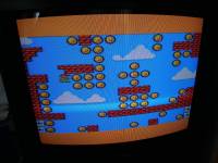
I noticed colored dots while loading the palette - I'm doing this outside of the VBLANK and this is probably a problem? Does writing to CRAM have to be during VBLANK so that no such arfetacts appear?
https://dl.dropboxusercontent.com/s/krm48urbp6jelmd/sms_engine_test.sms https://dl.dropboxusercontent.com/s/mrv36oiwlgwusg7/sgg_engine_test.gg |
|
|
|
|
|
|
| Unfortunately, those dots appear even if you do write to the color RAM during vblank. To get rid of them, you have to do your writes within a specific scanline range that places the dots sagely outside of the visible screen area. | |
|
|
|
|
|
| Is it possible to run games from SG-1000 on SMS II console? I know that SMS EverDrive can do it, but I am interested in modifying the SMS cartridge to upload a SG-1000 ROM to it - a combination of 2 EPROM 27C256 and 27C128 chips (PRG ROM 48KB). Is there any wiring diagram available? | |
|
|
|
|
|
| SG-1000 games will need a valid header to be added, which can be difficult. | |
|
|
|
|
|
|
So if I want to test my SG-1000 code on SMS, I have to modify it (add some boot code)?
My guess is Master ED patches the ROM to boot? |
|
|
|
|
|
|
|
you have to add a ROM header - look here: https://www.smspower.org/Development/ROMHeader
ED doesn't need to patch this at all, as the BIOS already has given control to ED's program, which doesn't perform any check. |
|
|
|
|
|
|
| Just adding .SMSTAG (WLA-Z80) in source code will allow SG-1000 ROM to run on SMS? | |
|
|
|
|
|
|
I would like to set the video mode 256x240 (PAL-SMSII) - is it enough to set Bit3 in Register $ 01? Unfortunately, nothing wants to work, maybe it is the fault of the emulators, which by default work in the SMS emulation v1 mode?
What do I have to do to get 30 row/240 line mode? |
|
|
|
|
|
|
You also need to set bit 1 of register 0. https://www.smspower.org/uploads/Development/msvdp-20021112.txt might be helpful. |
|
|
|
|
|
|
| Thanks, I didn't pay attention to that. Do I need to change the tilemap bass address? I was 3800 but I have to change the skrollY register to $ 20. Do I need to change the base address of tilemap to $ 3700 (then I can have skrollY register to $ 00)? | |
|
|
|
|
|
From the same document:
and
|
|
|
|
|
|
|
|
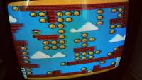
I set Bit 2 and 3 in REG02, I set Bit1 in REG00 and
copied the TileMap from $ 3700 - it only works on Emulicious, there are errors on other emulators and the background is not displayed. |
|
|
|
|
|
|
it should work in MEKA too, but in any case if it works correctly on the latest Emulicious I would say your code is correct :) |
|
|
|
|
|
Last edited by siudym on Fri Oct 07, 2022 9:12 pm; edited 1 time in total |
|
I noticed that the FUSION emulator is booting this ROM on PAL system correctly. But when I checked it on Everdrive on 2 different Sega Mega Drive PAL clones, the screen was displayed incorrectly (depending on the clone model it was displayed a bit differently).
Tested on SMS II PAL and works fine. 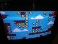
|
|
|
|
|
|
|
The MegaDrive VDP doesn't support the extended resolution modes, as it's a fork from the first revision SMS VDP, that had no such modes. |
|
|
|
|
Goto page Previous 1, 2 |