|
|
ForumsSega Master System / Mark III / Game GearSG-1000 / SC-3000 / SF-7000 / OMV |
Home - Forums - Games - Scans - Maps - Cheats - Credits Music - Videos - Development - Hacks - Translations - Homebrew |
View topic - GameGear-TV
 |
Goto page 1, 2, 3, 4, 5, 6, 7 Next |
| Author | Message |
|---|---|
|
Novaline
|
GameGear-TV
|
|
You might find this interesting.
I bet you would love one of these! http://hem.bredband.net/hensam/ggtv.rar |
|
|
|
http://www.smspower.org/dev/ggtv/ Oops! |
|
|
|
|
|
Novaline
|
|
If you would have given the pictures a minute of examination, then you would have noticed... This acctually works. Not the same board. No-one have to my knowledge been able to recreate this boards function. May it be that the pictures you linked to is incorrect? |
|
|
Last edited by Bock on Fri Aug 25, 2023 2:05 pm; edited 1 time in total |
|
In the directory Maxim mentionned, there's three (bad quality) pictures of the same Game Gear with the same board as your Game Gear.
I took those pictures a while ago. The schematic stuff are because people started working on replicating the mod, but you're right that noone got it to work perfectly as of yet. Notice your Game Gear is serial number B4U000038 and mine B4U000105. They are from the same batch given to developers. May I ask, where did you obtain it? Thanks for your picture btw. Mine are outdated and not of good quality. With your permission, I'll add your pictures in the same directory. *EDIT* My original photos were posted to https://www.smspower.org/forums/1413 |
|
|
|
|
|
Novaline
|
|
Well, first of all, it's not mine. Serial no, point taken. I see that the capacitors on this unit might be replaced by surfacemount components in your pictures. It belongs to a friend of mine. He bought it from a dude on eBay. Paid like $75 for it, postage to Sweden included. He dont use it much, because it's kinda valuable. (He collects GG stuff, and wont sell it.) He gabe you permission to use the pictures, but only if you can replace them with sharper ones the next time he takes the unit out of the box. |
|
|
|
|
Does he have reference of the auction url/number? Just for curiosity, to see the description. And, I may try to ask the seller from where does it come from.
$75 is a good price. I was supposed to pay $50 for mine but kinda got ripped off by the seller who got away with a $150 check (for a complex reason) and stopped answering to me. Anyway even at this price I would have bought it. It's not necessary to remove old pictures, all pictures may be informative so I'll keep the old pictures and add the new ones if they come. May I get in contact with the guy? I do also collect GG, maybe we could exchange a few things. Do you have problems quoting texts? (I wonder if this forum is easy to use for everyone). The starting quote BBcode was missing here so the quoted part of your message doesn't look like a quote. You can edit and fix your message if you understand the problem, else I'll do it for you. |
|
|
|
|
|
DJ
|
GGTV Info
|
|
If you look at photo 100_1489.jpg (ggtv.rar) from Novaline you will notice that there is anothe IC under the 315-5242 chip. Does anybody know what this chip is or have other photos of the GGTV board from the side.
I presume that there are at least 6 IC's on the GGTV board as you can see the following: IC1 - SEGA 315-5242 IC5 - 74HC175A IC6 - 74HC00A The board does not look terribly hard to make if we could obtain a few more details on the other chips and connections. IC1 can be obtained from SEGA system 18,24 arcade boards and IC5,IC6 are standard 7400 chips. I have had some limited success with getting the GG on TV but I have not got right colours yet. Does anyone have anymore info? |
|
|
Re: GGTV Info
|
The main problem is that it isn't known where various video-related signals can be tapped from on the GG motherboard. I have it on good authority that this has been figured out and a homemade solution is currently in development, we'll just have to wait. While I don't know the exact details, I can give a rough outline: The 315-5242 is DAC and video amplifier in the same package. It requires a clock equal to the pixel clock (5.36 MHz for the GG) and a active-low video blanking signal (to blank the display to establish the base for the black level of a monitor). While the 315-5242 supports 15-bit video (RGB 5:5:5) only the upper 4 bits of each are used (12 bits total) because that's the resolution of the GG palette. The video output of the GG comes from a multiplexed 6-bit bus; the 74HC175 is used to sample data so all 12 bits can be fed to the 315-5242. The 74HC00 could be used for a variety of things, most likely it combines the pixel clock and video bus multiplex signal to trigger the 74HC175's clock input. The 315-5242 could be implemented using a resistor ladder and amplifier circuit (a transistor or dedicated video amplifier), it has some extra functionality that is unused in GGTV and can be ignored. So you can assume somewhere on the GG mainboard are the following: - Six bit video data bus, multiplexed - Said multiplex signal to indicate what's on the bus - Active-low screen blanking signal - Pixel clock - Composite sync output While I can't say this is right, it fits with what hardware is on the GGTV board, and I've researched the 315-5242 in other arcade boards quite a lot. |
|
|
|
|
|
Re: GGTV Info
|
|
Actually I tried an RGB decoder on my european Gamegear (with classic component don't be affraid ).
I think there is only 4bits for color, see my little calcul: 4bits=16 values SO 16red x 16 green x 16blue =4096= Complete GG palette I built a working module with 3 4bits latch ( data pins c66 c59 c60 c61) each connected to an R2R DAC , I take T2 pin as Sync signal. The 3 latchs are driven by a 2->4 decoder connected on C75 and FB1 It give a stable image with red and blue correcly displayed but the green is corrupt. I think the latch are not correclty driven. I tried replace decoder by binary counter ( C75 as clock) but it dont work. Anyway I think the first part: Latch+DAC is correct. Any Idea? NB: on my GG the motherboard is different than all picture I see on internet. Maybe an old version? |
|
|
|
|
|
DJ
|
GGTV
|
|
Thanks Charles and Xavier.
No doubt you have seen Chris Covell's and Victor Kemps site on the GGTV. The photos on these sites (if there are correct) show the data connections as being 4 bit. Some of the inputs of the 7400 are tied together and the outputs chained to other NAND gate, so maybe this is just buffering some of the signals. Another thought I had for the 74175 is that they might be used for dividing the clock signal to make the pixel clock. The crystal on the GG runs at 32.2159Mhz so I guess the pixel clock (5.36Mhz) must be the main clock divided by 6? Xavier, there are at least two versions of the gamegear (old and new) that I am aware of. I bought a copy of the GG (both old and new versions) schematics a while ago and have been using these in my attempts at the GGTV. Working from the GGTV photos and circuit diagram I tried to match the up the GG connections to GGTV. These are only guesses but this is what I have so far. Old Version GG (1 ASIC) Pin 1 - C22/R13 (Data) Pin 2 - C23/R14 (Data) Pin 3 - C24/R15 (Data) Pin 4 - C25/R16 (Data) Pin 5 - T2 (Composite Sync) Pin 6 - T7 Pin 7 - T1 (CPU Clock) 3.58Mhz Pin 8 - T13 Pin 9 - T10 or T11? Pin 10 - T10 or T11? Pin 11 - C11+ +5v Pin 12 - C11- Gnd Pin 13 - T12 Audio Gnd Pin 14 - T8 Left Speaker Pin 15 - T9 Right Speaker T10 - T11 I don't own an old version GG so I then tried to match up the above connections to a new version GG. New version GG (2 ASICs) Pin 1 - C59/R54 (Data) Pin 2 - C60/R55 (Data) Pin 3 - C61/R56 (Data) Pin 4 - C62/R57 (Data) Pin 5 - T2 (Composite Sync) Pin 6 - T7 Pin 7 - T1 (CPU Clock) 3.58Mhz Pin 8 - ? Pin 9 - T10 or T11? Pin 10 - T10 or T11? Pin 11 - C6+ +5v Pin 12 - C6- Gnd Pin 13 - T12 Audio Gnd Pin 14 - T8 Left Speaker Pin 15 - T9 Right Speaker I can't find T13 marked on the new version of GG. It does not seems to appear on the board or circuit. I don't know how important this signal is and if it is possible to use a GGTV with the newer versions of GG. You sound like you are on the right track with your latches + DAC. I would be interested in looking at the circuit you have so far. |
|
|
Re: GGTV
|
That's an excellent point, and could be the case. My concern is how all the data for the 315-5242 is stored, coming out of just a 4-bit bus. It seems that you'd need either more storage than what's in the GGTV box (Xavier's figure of 3 4-bit latches sounds better) so it's a bit confusing.
I have to ask, where did you find the Game Gear schematics for sale? That's one of the 'must-get' items some of us have been looking for - currently we have the SMS and Genesis schematics, but others (Sega CD, Game Gear, 32X) haven't been found, if they even exist. :) |
|
|
|
|
|
|
|
DJ and Charles, thanks for the info,
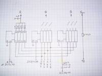
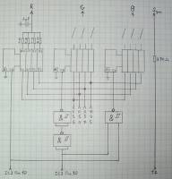
Indeed Chris Covell's and Victor Kemps site was of great help :) Here my output part schematic: 
latches are 3 x 74HC574 (unused part is for upper 4bits) or 2 x 74HC075 (less easy to find but take less space), plus if you can found the new 74Fxxx it's better. The DAC are typical R2R ladder, 2R can be from 390 to 470 ohm depending of your TV quality. Sadly R must be created by putting in parralel 2 2R resistors wich increase space. Maybe a simple Binary Weighted DAC wich require only 4 resistors can be used, but correct resistor value are rare if not impossible to found ( You can however try with rounded values)! For simplicity sake, test can be made by using an unique resistor of 330 ohm connected on the MSB of each latches ( with this configuration gradient 'll not be displayed but it's enough to test colours separation) For the command part... well it's not so simple, if you take signal from the missing C75 (new PCB version) inject it in "RED valid" and invert it into "BLUE valid" you obtain red/blue separation but green seems to be mixed in the 2 other colours: 
So a decade counter could do the trick ( first pulse red, second green and third blue) but my test with a standard 4017 give nothing, but according to DJ, 74175 + counter should be the answer. I'm sure It's just a timing problem! Another interresting signal is FB1 ( Fast Blanking ?). NB: And now a really bad joke, during my first test I used a 2->4 decoder driven by C75 and FB1 to control the 3 latches and I forget to connect OE of RED latch to ground, strangely the screen appeared nearly CORRECT??? I had just time to take a screnshoot: 
Since then I never obtain so good image. Call that Murphy law... [edit by Maxim: replaced huge image with clickable thumbnail] |
|
|
|
|
|
|
The DAC in the 315-5242 is made up as follows: color_bit4 -> 1.0K ohm resistor (4 in parallel) to common output color_bit3 -> 1.0K ohm resistor (2 in parallel) to common output color_bit2 -> 1.0K ohm resistor (1) to common output color_bit1 -> 2.0K ohm resistor (1) to common output color_bit0 -> 3.9K ohm resistor (1) to common output The common output goes through a filter, then to the R, G, or B pins to directly drive a RGB monitor. As mentioned the GGTV doesn't use bit 0, just bits 1-4. I was wrong, the 315-5242 does contain storage for the color data; it has a 16-bit latch (5 bits per color, 1 for another feature not used in this case) clocked by the pixel clock and cleared by the screen blanking input signal. So I agree with DJ's idea that the '175 is used for dividing the main clock to generate the 5.36MHz pixel clock. |
|
|
|
|
|
|
So after all a simple Binary Weighted DAC is enough, not a bad thing :) Just hope it's correct for TV impedance (75 ohm) because I don't know typical arcade screen impedance.
So my little Murphy accident is maybe a good think, It just give me an idea, I'll try it! |
|
|
|
|
|
|
|
IT WORKKKKKKK!!!!!!
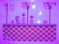
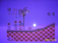
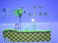
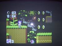
But don't ask me how.?!?! I just replace R2R DAC by Charles version, connect RED valid to C75, BLUE valid on FB1 and GREEN valid on a pin of IC2, and it work! Red seems a little too strong but maybe the DAC value are not perfect ( I use rounded value plus I need to filter the output signal) So blue tend to appear purple. Here with Sonic GG: 
And with Castle Of Illusion ( GG version but work in SMS mode): 
T10 and T11 must be tied, if not SMS mode looks horrible. My only guess is FB1 is set when blue data is yet avaible on data bus, allowing easy access to it, however we can't use it to blank latches after that, but it don't seem a big problem... I'll post a valid schematic as soon as possible. |
|
|
|
|
|
DJ
|
GGTV
|
|
Congratulations Xavier,
The GG photos look great. It looks like you have solved it. Funny how a simple R2R + Latches can do the same job as a complex GGTV. On my schematics FB1 is shown as an optional ferrite bead. FB1 connects through a 1K resistor to the X1 Crystal (32.215Mhz). C75 is shown as a junction between pin 10 U2 & pin 6 U3. Charles, Here is the link to where I brought the GG schematics from. (You wouldn't believe how many google searches I did to find them!). They are not the official SEGA schematics but have been reversed engineered. They are still fairly detailed. [/url] http://w3.trib.com/~rollo/ Back to the discussion on the GGTV pixel clock, if the pixel clock is running at 5.36Mhz what must be the speed of the R,G,B coming from the 4-bit bus? 3 x 5.36Mhz? 4-bits of R,G,B would need to be present (latched) on the 315-5242 inputs ready to be clocked by each pixel clock. Also, how did you calculate the pixel clock. I took 15.734Khz / (256 pixels across + 64 (video blanking,etc)) and got 5.035Mhz. I then rounded this up the the nearest multiple of the main clock, which would give 5.36Mhz. Is this correct? A 5.36Mhz pixel clock probably means there is about 340 pixels in total across the GG screen. |
|
|
Jan Solrac
|
weeeeeeeee
|
|
weeeeeeeeeeeeeeeeeeeeeeeeeeee...
impressive ! post your results guys!!! god bless u... lol |
|
|
|
|
I don't forget you ;)
I'll post the revised schematic this week-end. Thanks to DJ info, I improved the display quality and now colors are perfect. Since I did a mistake and take FB1 as Fast Blanking (wich give incorrect blue), I must use another signal as Blue valid, such signal don't seem to exist on GG board so I use a little trick, I take a signal very near and use RC filter to tweak it ( I know it's terrible) there is however a little problem, sometime glitch appear with certain colour combinaison, it's rare and very small but... its not perfect. Keep in mind it's a hack, I don't think the original GGTV use the same principle. |
|
|
|
|
|
Re: GGTV
|
Looks a bit odd, but they have a lot of interesting stuff!
The VDP is connected to a 10.738635 MHz clock, divided by two for the pixel clock of 5.369317 MHz. If you apply the CPU clock to pixel formula in the GG manual, a 5.36 MHz pixel clock gives a CPU clock of 3.579545 MHz which is known to be correct. Just mentioning it so you can see where I'm getting these numbers from.
That's right, IIRC both the TMS9918 manual and my timing document support that number. 256 pixels are for the display and the rest are horizontal sync, blanking, color burst, and the left/right border areas. |
|
|
|
|
|
Suggestion on "valid" signals
|
|
I think only 1 of the D-latches in the 74HC175 is required to divide the main 32MHz clock by 2 to create 3 clock cycles per pixel (32MHz / 2 = 15MHz = 3 x 5MHz - the pixel clock).
One of the NAND gates could then be used to create the missing "Valid_Blue" signal from the present "Valid_Red" and "Valid_Green" signals. Then use the remaining 3 NAND gates to combine the 15MHz clock signal with the 3 "Valid" signals to create the 3 latching signals for each of the RGB colours. All this depends on the exact operation of the "Red_Valid" and "Green_Valid" signals from the gamegear, but it's how I see it working. Oh, and never, ever, use 4000 series logic in MHz-speed systems. You're asking for trouble. I hope this helps with the final solution. |
|
|
|
|
|
|
|
As promised here the new schematic:
****************************************************************** IMPORTANT: This schematic is for the 2 ASICS Version! ****************************************************************** 
***************************************** IMPORTANT: Use at your own risk! ***************************************** The latches can be 3 x 74HC574 (put unused input to ground) or 2 x 74HC075, Filtering 1nF capacitors are here to "soften" output signal ( A lot of new TV don't appreciate ladder type signal) and are optional. DACs are now Binary Weighted type as the original GGTV, perfect value are: R1=2Kohm R2=1Kokm R3=500ohm (2x1k in parralel) R4=250ohm (4x1k in parralel) All resistors must be 1% precision or better! For those who want gain space rounded value work but can decrease color quality: R1=2,2 Kohm R2=1,2 Kohm R3=560 ohm R4=270 ohm Give acceptable result. T10 and T11 must be tied together for SMS mode. Now I must be clear, this device work, as you can see 
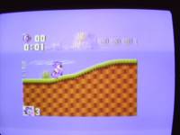
( Don't panic, the blur effect is on the screenshot only ^^! and blue is no longer purple ) BUT, it must be taken as a quick and dirty method, I am sure than the original GGTV use a far better system to control the latches. I simply found than some signal of IC2 can be used as substitute, it work pretty well with Red and Green, but sadly Blue was nowhere to see, so I tweaked a similar signal with RC filter and use it. As result the schematic is really simple, but I found two drawback( only due to blue control): -1- Some rare colour combinaison shade the blue ( for instance Dark blue on bright white sometime become near black like the SEGA screen on Sonic GG) -2- Sometimes, If a game use a 1 pixel by frame horizontal scrolling and/or an interlaced display, graphics glitch can occur ( jungle waterfall in Sonic GG). So consider this system as a temporary solution until better blue control was found, or original GGTV was completely reverse-engenired. NB:
A really bad habit of mine ^^! In fact, I always forgot than CD4017 work speed depend of it voltage.... with 5V only it's 2Mhz, in the best case! |
|
|
|
|
|
|
|
Shouldn't that be in the "Documentation" section ??? I just love that 74xxx family... we can do everything with them...
Excellent work! I can't wait to build one for me... |
|
|
|
|
|
|
|
Thanks Jan,
as I said this system is imperfect, it must be considered as a "work in progress" rather than final document, I'll put It in documentation section when I',ll be complitly satisfied. "Asynchronous" give us some interresting idea, using an 74HC175 as clock divider is quite unusual but possible, obviously SEGA use a lot of hack itself, his SEGA 315-5242 part is a good example, I think a large part of it internal circuit is not used in the GGTV, SEGA must had extra stock of it from their arcade PCB and tweak it in the GGTV, there's no small profit...
Indeed, they are wonderfull toys, but can take quite space, even in CMS. If somebody want put his homemade GGTV in the battery area it's pretty difficult. Once finished, maybe we can try to put all the logic in a single GAL (minus DAC), homemade burner are really easy to build. |
|
|
|
|
|
Final version
|
|
VICTORY!!!
The final and stable version of the GGTV is completed, now colours are ALWAYS perfect both in GG and SMS mode without any glitch, the only drawback is you need one more IC 74HC00, to NAND red_valid with green_valid and use the result as blue_valid, simple isn't? So we no more need to tweak pin 44. Now a little question, the schematic is really simple: 3 x latches/DAC , 1x NAND. Then why, WHY SEGA use such complex component for this simple task? I mean, there obviously no need to handle pixel clock or other complex operation, then WHY? I'll soon post a complete "How To" document. |
|
|
|
|
|
New screenshoot
|
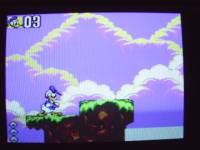
Here some screenshoots to wait my doc:

THAT is parallax scroll ! 
One of my all time favorite game... 
No more glitches in the waterfall ! BTW: It seem there are some free space under the GG cartrige connector, maybe the GGTV can be fitted in ( instead of in the battery area). I'll try to draw an adapted PCB mask ( for those who can burn it). |
|
|
|
|
|
Phredreeke
|
|
| NAND Red and Green to get blue? How does it produce magenta or cyan, that contains both blue as well as red or green? Or black that contains neither color? | |
|
|
|
I speak of VALIDATION signal controlling the latches ( the clock pin), not the digital input or analogic output!
Take a look at the last schematics to see what I mean. |
|
|
|
|
|
|
|
Congratulations to all those involved with this!
I was actually working with Victor Kemp on this for quite a while a few years back, so I'm quite glad to see someone finally cracked this. I've hoped since the GG's release that someone would finally figure this out. Great job! I noticed some changes were made after that final schematic was posted...is there a newer version of the schematic that will be posted to reflect this? Great new board format, folks! This is my first post on the new one. I guess I haven't been here in a while. :-) -Rob |
|
|
|
|
|
|
Yes, I did a lot of modification/improvement since the last schematic. However I have some stability problem with my second prototype so I want work on it more time before I post a correct documentation. Take note the actual posted schematics give incorrect blue. BTW, Victor Kemp homepage was a goldmine for us :) |
|
|
|
|
|
|
|
Good job, Xavier! I can't wait to do this modification myself. (But first, I have to get a second Game Gear and an RGB monitor. ;-))
Could you at least tell us what you have changed since the last diagram (and NAND modification), so we can get started with this project quicker? One last thing, in those final screenshots above, I see thin vertical lines all over the first two pics (and a little bit in the 3rd pic.) Are those artifacts from the latches? Can they be eliminated? |
|
|
|
|
|
|
|
Here the final schematic, at least I hope ;)
Read carrefully all info, because I did a lot of modification, even on DAC value ( the previous has too high output) ******************************************************************************************** IMPORTANT: This schematic is for the 2 ASICS Version! Sorry, I don't own a single ASIC GG so I can't identify the pin 10/30 substitute, but take a look at Victor Kemp and Chris Covell homepage to see how to connect the data bus. ******************************************************************************************** 
***************************************** IMPORTANT: Use at your own risk! ***************************************** Power supply are 5V with an average current of 30mA, so it can be extracted from the GG without too much risk ( I did a test during 2 hours without abnormal GG overheat) Of course you can use an external power supply, simply put the ground in common BUT DON'T connect 5V GG with external 5V or else BOOOMMM! Latches MUST be 3 x 74HCT574. Filtering 1nF capacitors are here to "soften" output signal ( A lot of new TV don't appreciate ladder type signal) and are optional. Depending of your TV, you can increase it's capacity up to 10nF, but too big value will blur the display. DACs are Binary Weighted type, perfect value are: R1=2,2Kohm R2=1,1Kokm R3=550ohm (2x1,1k in parralel) R4=275ohm (4x1,1k in parralel) All resistors must be 1% precision or better! For those who want gain space rounded value work with pretty good result: R1=2,2 Kohm R2=1,1 Kohm R3=560 ohm R4=270 ohm With such values we obtain typical 1V/75ohm TV input. NANDs MUST be 74HCT132, ONLY Schmitt Trigger type work! Each ICs MUST have a 100nF capacitor between all their power supply lines. You must connect the 4bits data bus between each resistor (R54 to R57) and his associate capacitor. For SMS compatibility you must tie together T10 with T11 but i'll affect the LCD display so use a switch, not a simple wire. And here some new screenshoot: 
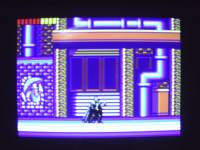
This game use LCD blur effect to display fake transparency, of course on TV it fliker like on emulator :( 
Such a cool game!
Yes, pretty easy to eliminate, give me a better digital camera, it don't come from the TV screen ;) Seriously, the sole default I found is when GG display dark red, very small black vertical line can appear on the red, but you must be at 10 cm of the screen to see it. I'll write a complete article for the documentation section but you can already work with this info. |
|
|
|
|
|
|
|
Just to clarify, since there seems to be some confusion: you're outputting RGB+sync, but it's at NTSC/75 ohm specs so it'll display on any TV with RGB inputs. You don't need an arcade/RGB monitor.
TVs in Europe have SCART connectors so that's easy, TVs in the US generally don't have any RGB input options which is silly. Am I right? |
|
|
|
|
|
|
|
Yes, you are right.
Some precision, video can be sent to TV or monitor via: - separete RGB+Sync, such system give the best image quality but require 4 wires. -Composite video, in this case all signals are mixed according to the country format ( PAL, NTSC, SECAM and the rare MESECAM), it take only one wire but the video treatment decrease the image quality. In the worst case video is sent via RF and the resulting image is horrible. -S-Video is an alternate system wich require two wires and give far better result than Composite video. All this signal must be 0,7 to 1V with 75ohms impedance, Vertical synchro can be 50 or 60HZ ( beware some old 50 Hz TV can't handle 60 Hz signal) and horizontal synchro are 15kHz. The signal created by the GGTV is pure RGB+Sync 60 Hz. VGA monitor are RGB but NOT directly compatible (VGA horizontal synchro is 30 kHz minimum). So in Europe simply use your TV scart ( put your TV in RGB mode with your remote control if possible or connect 5V via a 270 ohm resistor to the scart Fast Blanking pin to force RGB mode). In USA use either an analog RGB monitor ( old ATARI or AMIGA monitor just work fine) or an RGB to Composite NTSC or an RGB to S-Video adapter. In Japan, I know they now use SCART but with a different pin organization. For better info on scart, take a look at: http://www.gamesx.com/ Avoid true arcade monitor, they are expensive, not always easy to use, and even dangerous because they are often really badly isolated!
They really have my sympathy :( |
|
|
|
|
|
Some corrections
|
|
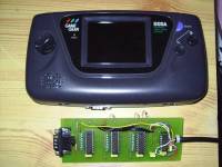
I build a portable PCB version in order to test the GGTV on a lot of different TV.
After tests with some TV model here new result: 1) Video level is yet a little too high for some TV, if your screen is too bright simply put a 120 ohm resistor in parralel ( or instead) with each 1nF capacitor ( it'll reduce light by 30 %). 2) The system is really sensible to static ( even with the Schmitt Trigger) , so you MUST use pull-down resistor of 1Kohm MAXIMUM on each video and control wires the most near of the GGTV ICs. My actual PCB is 6cm x 13cm, far too big to be inserted in the GG........ So, I use a DB9 connector to output all the signal on a single connector, therefore I can use my GG without the GGTV attached. To connect GG and GGTV, the best way to avoid static is by using a 8 wires shielded cable of 50 cm BIG MAXIMUM, longer cable give inpredictable result. And now a little question, since GGTV is name of the official SEGA version, maybe we can found a name for our homemade version, GGRGB don't sound really well, any idea? |
|
|
|
|
|
Kaneda
|
|
|
RGGB ?
TGGV ? |
|
|
|
| "TV Gear" is pretty meaningless but sounds cool. | |
|
|
|
|
|
|
BBGGTV? (BB=bare bones)
PMGGTV? (PM=poor man's) or how about just GGTV since Sega isn't making hardware anymore? ;-P |
|
|
|
|
|
Re: Some corrections
|
How hard would it be to route the video signal out through the EXT port, for those of us lucky enough to have a G2G cable and don't mind sacrificing it for the cause? Not that I have one of those :( |
|
|
|
|
|
|
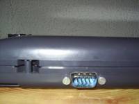
Possible, but highly NOT recommended, I can imagine tons of interresting applications with the EXT port, it's a pity to destroy it. See how I output signals: 
I use a simple DB9, a classic and robust connector. 
An image of my second PCB proto , DAC resistor are mounted vertically "à la japonaise" to gain space, pull-down resistor and bright reducer was later added on the solder side.
It sound great, I'll use it :) |
|
|
|
|
|
Stop the press!
|
|
OOPPSS, Sorry for those who begun to build their TV Gear with my last schematic, but I just found ( and corrected) a HUGE bug in the red command ( the dac part is correct ), I'll post a new schematic ASAP.
Since I don't own a true SMS, I couln't compare real colors until a friend grant me its one ;) On the bright side, colors are now even more beautiful :) It can seem strange, but SMS game display seem a little more "vivid" with the TV Gear, I suppose its video level is stronger than the original SMS. |
|
|
|
|
|
Update
|
|
Hey Xavier,
Just seeing if you have an updated schematic/documentation with your fix for this yet. I remember you mentioned you were working on a full docuentation for it. :-) Thanks again! -Rob |
|
|
|
|
|
So little time and so much to do...
|
|
Errr, sorry everyone, I'm really overbooked this days, I'll try to post the good schematic before this week end, but I can't promise you ^^!
Now since I have difficulties to take good screenshot of the GG pcb, if someone can post very clear picture of the motherboard, in particular the 2 asic part, it'll be of big help :) To davidleeroth sorry to be so late... Sadly there no means to identifies the IC2 pin 10 and 30 equivalent on a 1ASIC version but to test or find a schematic of the two version and identifies the pins of the 1ASIC version by deduction ( I highly suspect pin10 to be an alterate pixel clock and to be T13 pin on 1ASIC version). |
|
|
|
|
|
|
|
Was the 2ASIC the Majesco version? Or did Sega release 2 models of GG? Sorry, I know probably everyone on this forum knows this but me, lol.
-Rob |
|
|
|
|
|
new TV Gear schematic
|
|
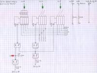
Here we are, ...after some time..., the new TV Gear schematics.
******************************************************************************************* IMPORTANT: This schematic is for the 2 ASICS Version! Sorry, I don't own a single ASIC GG so I can't identify the pin 10/30 substitute, but take a look at Victor Kemp and Chris Covell homepage to see how to connect the data bus. *******************************************************************************************  ***************************************** *****************************************
IMPORTANT: Use at your own risk! ***************************************** As I already say, the ancient RED control was wrong, Pin30 is simply the BLUE/GREEN control and Pin10 seem an altered pixel clock so I tweak it to select RED correctly. RC filter can appear primitive, but it work perfectly. Take attention to 2 points: - the 3 green resistors are the output level limiter, a good average value for TV is 220 ohm but you can modify it if you think the display is too bright or too dark. -the red resistor allow you to adjust RED/BLUE separation. Since its exact value is really hard to find, I highly suggest to use a variable resistor ( 1 or 2 Kohm), start a game and adjust it by your own (try to not short cut the gate output for too long). I'll try to find the control line for the 1 ASIC version, but it can be difficult... Some people asked me if I can build a pcb version for them, since it seem to be a perfectly stable ( at last) version, it's possible (but a little complex to manage). If really a LOT of people want pcb version, contact me and I'll see what I can do. Message in french: Je pense que je peux en fabriqué pour les gens résidant en France, les couts de fabrication+frais de port+rémunération décente sont à étudier. A partir de 10 piéces la plupart des founisseurs de composant proposent des ristournes, on peut ainsi économiser surtout sur les boitiers et les connecteurs, piéces souvent couteuses. Par contre, la logistique qu'il faudrait mettre en place si fallait que j'assure la pose d'un connecteur dans la GG me semble beaucoup trop importante. Les gens fachés avec leur fer a souder vont se sentir seul... Rappel: le montage marche sur une GG 2 ASICS ( premiéres générations), mais il n'y a aucune garanti que sa marche sur une 1 ASIC ( 199X ?). J'invite donc mes compatriotes intéressés a me laisser un message, s'il y a au moins 10 piéces je les fabriquerai. Xavier |
|
|
|
|
|
Re: new TV Gear schematic
|
I'll send you one free of charge if you want. Contact me. In french, you discussed producing several of them. I'd surely be interested, other people also very probably, but we'd need an approximate price. To be honnest I have no idea if such board would cost $5 or $100. Price will certainly affect the target audience. Maybe you could make a rough estimate of that. |
|
|
|
|
|
estimated production cost
|
|
A *ROUGH* estimation of TV Gear build without case is 45 euros ( 58 $,
32 GBP) shipping charge include ( for now only in France with "Coliéco"). It can take the form of a 60cm cable ( without connector, you are free to use anything you want for GG connection) connected to a TV Gear board and ended by a 1,5 meter scart cable (peritel) for a total of 2 meters cable. To reduce shipping cost I can't include a case for the pcb (maybe if i found a really flat case...). Of course, you can add a case later ( an old SMS cartridge case for instance). I'll build a prototype with this setting for my own use,and post a picture of the device ASAP. After that, people interrested can contact me. Xavier |
|
|
|
|
|
|
| I'll try to build this by myself soon. But Xavier, I have a question. The only ICs I can get ahold of are 74HCT574P and 74HC132P. Do both of these have to be 74HCT versions? And does anybody know what that extra P on the end of the names mean? Could they be used in the GGTV circuit? | |
|
|
|
|
IC reference
|
|
Hello Chris,
to make it simple: -NEVER use old 74 TTL familly (too much consumption). -AVOID 74LS family (limited output power) -You can use and mix HC, HCT, and F famillies ( and you can safely ignore the extra final letter it's for builder reference). Plus, take as habit to always use socket with your IC, so in case of problem they be easylly replaced. Remember to put a decoupling capacitor ( 100nF) between each IC power lines ( VCC and GND). Good luck to building it :) Xavier |
|
|
|
|
|
|
| I want one! :) (Sur Paris) | |
|
|
|
|
Cost
|
|
I definitely want to buy one. Cost isn't really a big deal, considering I've been willing to pay a couple folks WAY more than that in the past to get one of the official Sega dev GGs before (never did complete those deals). Can't wait to hear the results. :-)
-Rob |
|
|
|
 |
Goto page 1, 2, 3, 4, 5, 6, 7 Next |


