|
|
ForumsSega Master System / Mark III / Game GearSG-1000 / SC-3000 / SF-7000 / OMV |
Home - Forums - Games - Scans - Maps - Cheats - Credits Music - Videos - Development - Hacks - Translations - Homebrew |
View topic - New Master system 2 mainboard
 |
Goto page 1, 2 Next |
| Author | Message |
|---|---|
|
New Master system 2 mainboard
|
|
Hey guys, I found this site when i was in year 9 or 10... so 2001/2002
Before i sold off my original collection. I remember searching and downloading every master system rom back then.. before torrents... and documenting them all with what size the game ROM was etc. One of the only easily downloadable things back then on dial up internet. Everytime I look up anything master system related, it brings me back here so i signed up to post :) I decided as a project to learn Kicad, and because i find it enjoyable, why not make a master system mainboard. It was on my mind until i found OpenTendo and NesEssity - then i thought yep, I'll do it.. the schematics are already online... it won't even need reverse engineering. I figured I'd sort of blog the progress here, that way people can have their input etc.. and help fault find. SO the board is based off the French model, this seems to have the least components. My guess is the video circuit used caused the other boards to be extremely noisy. This one has very few components and it's the easiest to recreate, plus we want to use our own video circuits. I figured I could make the board as small as possible, with a bare patch of PCB and some solder pads to add what ever video circuit you want. So just 4 pads for RGBs, I'm quite interested in an LT6557 I was recently playing with and the THS7316 and have both on hand so I don't want to commit components and footprints to specific RGB amps. I managed to track down the proprietary parts required before starting of course. So we have a master system 2 VDP, with the master system 1 I/O controller that was retained on the french model 2. So far pins are all numbered, symbols are all done, and corresponding footprints have being found/ made and associated. Labels for IC's are all done. I started with the VRAM / VDP interfacing. It's not as neat as Segas, I am unsure of how they managed to get theirs so tidy.. but mines not a mess at least. I've cross referenced with this: https://www.smspower.org/forums/10098-3155246And3155330Pinouts The BIOS took me a while to decide on, I like the idea of the little square type ones but for less of a headache I just went the 32DIP package AMD 29F010 as used in the BIOS guide on this site. Someone hacked the cool protoype intro just 5 days back to work with every game so I'd like to use that on the board. I may need help to clear up some confusion on it as well with varying pin names and numbers used on the different schematics (often you have to load up a different version for reference because they've been photo copied a lot, and hand drawn) Progress will likely be slow, it took all weekend to figure out Kicad schematics, symbol/ footprint associations etc then a couple of hours to lay it down which I've had to make several adjustments already. One mistake can really consume a lot of time to rectify. For now I'm quite comfortable making quick adjustments and changes and getting them to reflect on the PCB. Expect plenty of mistakes! These schematics are like the book "wheres wally" I will obviously need to return and make a lot of changes when the ground and power rails, and other components are laid out etc.. You can already see pins buried behind both layers traces that need to be "dug out" later 
|
|
|
|
|
|
|
| z80 D lines were copied and pasted off another IC, Pin numbers are D0 to D7 as pin 1 to 8. Corrected, Interfacing I/O controller and thats it for this arvo | |
|
|
|
|
Last edited by L10N37 on Wed Aug 26, 2020 9:02 am; edited 1 time in total |
|
incorrectly labelled all NMI pins as NMI, corrected label NMI from P22 of VDP: relabelled as NMI-IN along with P50 of cartridge slot. This has a 4k7 pullup and pause switch on it. The switch on the schematic was marked as reset instead of pause. Also corrected.
Broke out Clock and crystal in/out pins from VDP to open area for it's components down the track. Look like theres enough room without any major changes to squeeze components in here close to pins. Labelled and broke out R / G / B / C sync and Audio lines, away from, and on the opposite side of the clock line Realised I need to do the 50pin cartridge footprint/ controller input schematics etc before continuing any further. Kicad gives a fairly good indication of best placement by moving IC's/ components around, rotating them etc until you find a location that looks like it'd be the cleanest position for laying tracks. Without the the "this one goes from here to here" lines of the controller and cart footprints I could ultimately waste a tonne of time routing tracks that need to be re-done once those sections of the board are implemented. It's probably time to start laying down filter caps etc I go as well. started roughing out the Z80 placement. Not 100% sure of this location 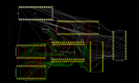
|
|
|
|
|
|
|
|
It might be worth baking in the "jailbars fix", although I guess that's still a bit of a work in progress with the PLL sync stuff.
After hacking the M404 BIOS I went on to fully disassemble it: https://github.com/maxim-zhao/smsbioses/tree/master/M404 so it should be possible to fix some of the bugs in it and add in proper cart detection; alternatively a micro-BIOS could be used to boot the game much faster (removing unnecessary delays and checksumming). Either way, swapping out the BIOS should be easy. Are you planning on supporting cards or just cartridges? |
|
|
|
|
|
|
I just want a switch on it to go between BIOS/ Built in game and a hardwired everdrive. We currently have 145 of around 279 PAL releases.. quite a few rares/ desirables and I don't want to "wear them out" I suppose i could just release it publicly once its done so that everything is known as working and people can do what they wish with the board. Will look into the pause on controller hack too. Although I've always figured it would be easier to just run a momentary switch up to your controller on an additional pair of wires with a little 2 contact plug type thing. |
|
|
|
|
|
|
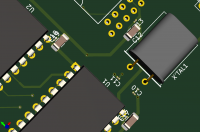
Is this you ?? I’ll be redoing the footprint for this 10F1L he’s using as it’s 28pin and exact match of factory one |
|
|
|
|
|
New Master system 2 mainboard
|
|
The early PAL SMS1 uses 74-series logic D flip-flops to generate the 10.6MHz clock for the VDP and the 4.4MHz sub-carrier from the 53MHz XTAL externally to the VDP.
So you have the building blocks to generate an external and in-sync VDP and CPU clock if you wanted to. No PLL required. |
|
|
|
|
|
|
No, I re-did it in response to a question on the Discord channel: https://discord.com/channels/489712349012295682/489712349012295684/7457775890161...
Some other notes: * Due to a sort-of bug, the wibbly-wobbly Sega logo is in different colours but these get replaced with the white/cyan of the later animation. * It doesn't turn off the screen when booting the game so you see some glitches * It doesn't tell the game what slot it booted from (port $3E value left in $c000) so some games will hang All these are easily fixed. |
|
|
|
|
|
|
|
Confusion over BIOS is sorted, it was just quick glances. Looked properly. They’ve just marked pin22 as A15 instead of output enable on the RGB schematic. It’s the same.
May leave the 32 pin DIP on the board for BIOS. Waiting for confirmation that a cheaper type flasher is compatible with that IC. It’s ultimately just going to be what ever is easier and cheaper to obtain, but once I run traces I’m not going back . Things from China are taking 3 months to get here. Other countries cancel orders altogether. As the sega IC‘s slowly make their way here I decided to look into the RAM. I was really confused as to why they used Sanyo LC3664AL-10 for system RAM and the NEC D4168 x 2 for VRAM on the segas I’ve opened up. Read the RAM page on this site and confirmed that... There’s no real reason. 8kb SRAM isn’t that easy to get now, not off main electronic places. They don’t stock it. The NEC originals are way overpriced. ** actually : http://www.farnell.com/datasheets/63505.pdf http://www.farnell.com/datasheets/1837125.pdf http://www.farnell.com/datasheets/2865453.pdf It’s not hard to find (but this is slower access times) search 64k not 8kb lol **** Searched around a bit and found this https://media.digikey.com/pdf/Data%20Sheets/Cypress%20PDFs/CY7C185.pdf This should suffice for my RAM/ VRAM. There’s more 28SOJ packages floating around of this IC but I managed to track down 28DIP purchase for a great price. High chance the German seller cancels. Spent a few hours tidying up the schematic, added 50p cart slot, all labelled. Components for 4 of 7 ICs are foot-printed and labelled along with pause and reset circuit. Started a components list document whilst going through each IC. Found a suitable/ more easily obtained replacement for the pause circuit diode. |
|
|
|
|
|
|
|
Early knock off today.
done some research on capacitors. THT type are far more resistant to heat. A non issue in this case. They automatically lay a spot down on both sides of the board you cant pass with traces. SMD will only affects one side. Not really an issue either. Was thinking just keep it THT until I noticed the SMD capacitors had a 10% tolerance and the THT had 20% This means a 10uf cap could actually be anywhere from 8 to 12uf whereas the 1206 would be between 9 and 11uf this is more than likely absolutely negligible, but higher quality is higher quality. Changed them all to a 1206 footprints for the 10uf and 0805 footprints for the 22nf (which also come in 0603/ 0402). *** found these: 0402YC223JAT2A with a 5% tolerance so using 0402 footprints for this value Also: Walsin, McPro, Kemet made sure it was possible to hand solder: *** We are looking at about 25cents each for the THT and 40 cents for the 1206 SMD type at the 10uf value. No biggie. Somewhere above I called the decoupling caps/ bypass capacitors "filter caps". My mistake. IF I don't get hassled this arvo for a few hours I will finish the schematic (controller circuits, power circuit etc) Then onto the fun part. Measuring out a board cut and squeezing everything together/ running traces :) |
|
|
|
|
|
|
Is there a diode involved with pause? I thought the z80 nmi pin was just held high through a resistor and the pause button pulls it to ground when its pushed. The reset circuit uses a diode.. but thats just to quickly discharge the cap when power is removed. You could probably replace all of that with a modern reset generator chip |
|
|
|
|
|
|
|
Although kicad is very powerful software, it is free. Free software always come with its annoyances
Schematics are pretty fussy, you can have a wire visually connected and lablled but until the junction point shows, its not actually connected. It's giving me drama running tracks to the 0406 footprints, not allowing me to run them at all etc, having to find weird work arounds. An example is shown where I can't link 2 earth pins. No big deal as i can run them both to the earth plane separately later. Might show as a false DRC check. Looking up parts and making / finding footprints is time consuming. A lot more changes and still not that much progess on the schematic. Getting there. Decided on a Crystal as a standard 10.7mhz HC49-U THT (ebay, mouser, ali express) Pal models = 53.203424 / 5 = 10.640684mhz, French RGB = 10.738635mhz direct at VDP 10.7mhz being a standard component, it's easy to obtain part and its frequency slots right in there. A teeny tiny on the fast side but not as much faster as the French model. Time to squeeze in some components in between completing the schematic. one entire side of the VDP is locked in other than ground/5v and EXM1/2, Schematic is a bit of a mess but you get that. Fingers crossed no major changes need to be made it's a pain in the ass If I've missed anything so far. Have had a couple beverages and lost track of time, time to get off the computer :) In reply to above: reset not pause, i keep mixing them up as there's only a pause button which no other console has, consoles have reset buttons. (can already see something dumb i've done with the xtal traces lol, no need for that) **Also aware on the BIOS IC A15 is to be grounded with other address lines above A14 (can’t remember on this IC) and EXM2 is output enable pin for bios 

|
|
|
|
|
|
|
|
Something really bad is on television that women like to watch which gives me time to ponder
Came up with this Pause button idea which is ultimately a new mod. We take the unused pin 5 of master system controller on the DB9 and this becomes the additional momentary tactile switch/ button installed in the controller across to the NMI circuit. Swap the cable out for a replacement megadrive one with the additional wire My current controller when I do use the master system (as I have a bag of genuine controllers and none are quite right, they need new rubber pads) is a modified clone nes console controller. It was in brand new condition and had an oddly sized DB9 on it. Just cut some traces and sanded them back / tacked on an offical master system cable, got to the final boss of sonic with a few lives left on my first try of it. Couldn’t get close as a kid. Master system controllers aren’t a strong point lol 
|
|
|
|
|
|
|
Not to rain on your parade, but this isn't a new mod. TheNameOfTheGame already did the same thing with a modified SMS++. There's a downside to this approach, which is that you can no longer read MD pads. Most of the time this doesn't matter, but being able to read start is useful for GG2SMS hacks. |
|
|
|
|
|
|
I’ll look into it after work, if you could reference this i would appreciate it. My understanding was the additional inputs on the megadrive were dependant on the additional wiring of pin5 on the DB9 being +5v , which the master system doesn’t provide. Start doubling up as another button on the SMS pad, where as start is an additional button altogether on the MD. It should still work with a megadrive controller but it would be expecting +5v on Pin5 not an NMI circuit ?? |
|
|
|
|
|
|
|
Also with the VRAM bus to VDP being so neat on the master system I done some more research and found that Address lines and Data lines (this should have being obvious) are all the same
Scattering these is common practice but it wouldn’t match the pinouts for the schematic which would make fault finding tedious. This means all the Bus’s Data and Address lines can be switched around for super clean trace routing. Also the German seller cancelled the cypress SRAM order. Found these other ICs which should be suitable. I’m still assuming having the DRAM refresh pulsing through to the internally disconnected PINs (as refresh isn’t required on SRAM) shouldn’t hurt functionality 
|
|
|
|
|
|
|
Sorry, I perhaps wasn't clear enough. Your understanding is correct, I was just pointing out that having access to the start button on MD pads makes GG2SMS hacks much easier to pull off. But you can't do that if you're repurposing the TH line as your pause button. Here's TheNameOfTheGame's work that uses a button tied to the TH line: https://www.smspower.org/forums/17693-SMSModifiedSketchForGG2SMSAndAutoFire Personally, I think that using use the up/down SOCD combo is best for the pause button on SMS pads. It doesn't break anything, including detection of MD pads: https://www.smspower.org/Development/JoypadPauseButton |
|
|
|
|
|
Last edited by L10N37 on Sun Aug 30, 2020 2:27 pm; edited 1 time in total |
I will look into this and see if I can incorporate it onto the board when the time comes. **it still shouldn’t block megadrive controller detection though. A megadrive controller plugged into a master system works fine. You just don’t have the additional inputs (which are not needed on sms games) without the 5v line. By extending the pause circuit line into a Master system controller we aren’t interfering with anything as the line (pin5) is not used by the megadrive controller when plugged into the SMS. ****yep gotcha, using the brazilian schematic for controller inputs as its most legible, 16 x 2200pf EMI filters + 2 x 270pf EMI filters, 3k3 resistor on TH and TR lines and a 22nf bypass cap on VCC pin5 for each controller. I hadn't looked into this yet and it was stupid to not realise you obviously need power hooked into the circuit it just isn't tied in on the bus. Just labelled, and I wasn't thinking. I will look into the mod and adjust the schematic to suit for the simultaneous U+D combo mimicking the pause with the gate IC's |
|
|
|
|
|
|
|
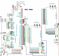
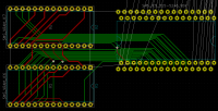
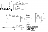
New VRAM/ VDP Bus interface
very crude, yep got off the ubuntu/ KDE Plasma laptop and got serious on the desktop, SERIOUSLY microsoft painted the Sh** out of this. I tried printing and paper IRL but couldn't ctrl+z This is far neater once tranposed and updated on schematic, especially considering ground and +5v planes. No point attempting to recreate a motherboard if it's a sloppy mess. That ONE VIA really, really upset me **those vias 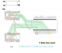
|
|
|
|
|
|
|
|
Now we can keep all our tracks to one side of the board between IC's
This should make for far better ground and power rails Won't be doing an udpate until I make proper progress... time for beer 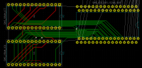
|
|
|
|
|
|
|
|
So thanks to Wafer he made me realise some things about the controller inputs, the pin-outs dot R U site had the 5v pin 5 pictured as not connected on the DB9.
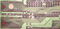
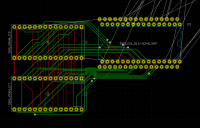
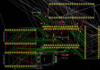
I haven't really looked into it further but with it possibly being used by gamegear hacks or whatever, I decided to integrate the Pause hack. Got my head around the pause hack as something as follows: 4001 NORGATE U+D OR L+R combination P1: Pin 8/9 (or input E&F) are outputting simulated pause button press signal on Pin10 (or output "L") when both (Input E/F) are pulled low (due to new button added to controller pulling both low simultaneously with opposing directions on the D-pad) ,simulated pause button output signal is sent across to pin 22 on VDP (NMI-IN) P2: same as above but using a different input/ output bank (A+B output on J or Pin 1/2 outputting on Pin10 ) Here you could use G+H out on M, or C+D out on K alternatively 74HCT02D As above but using a single output pin for both inputs. P1: Pin 2/3 P2: P5/6. Output on Pin13 to NMI-IN on VDP. Will not be using a diode as not required unless pause button is hooked onto the board along with the modified circuit Decided on the latter here. Because I'll save 20 cents lol (... because its a slightly smaller SOIC 14 footprint.) I ran out of room on my Schem sheet which I'm tidying up as I go. It won't stay a mess. All that matters are pin numbers and labels so I'll be getting rid of all the visual stuff (bus lines/entries) and tidying it up. I now need to change some labels to hierarchical labels as I've moved to a new Schematic sheet. Notice I am overshooting deliberately and creating junction points as absolute confirmation the connection is made. Previously when transposing to PCD from Schematic it wasn't giving me Ratsnest indicators for pins where abouts until overshooting the pin with the wire. Kicads been giving me a lot of dramas, constantly getting warnings about using old libraries (they were packaged with the install) and needing to revert and acting like its saved me from wasting my time but causing more time wasting re-doing things. Some progress shots, keep in mind once it's all done you do copper fill zones with thermal relief around ground pins to fill it all in. 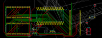
|
|
|
|
|
|
|
| I recommend that out of the two you use U/D. L/R could cause GG2SMS hacks to incorrectly identify a hacked pad as though it were an MD pad. You could add solder jumpers for both input pairs, so you can decide later and change it relatively easily. | |
|
|
|
|
|
|
Just had a thought on this: no matter what pair of inputs you use, the SOCD pause mod prevents you from using the extra buttons on six-button pads, because they pull all four directions low when you poll the extra buttons, so they'd trigger the NMI every time they're polled.
You could workaround this by using the TH line to disable the mod, so it only reacts to real SOCDs on standard Master System polls, and not the fake ones used by the Mega Drive pads to ID themselves. That way, it doesn't matter whether you use U/D OR L/R as the trigger. (Yeah, you guessed it, I've got a ROM hack that uses those extra buttons) That just leaves Saturn pads, which would need a manual killswitch for the mod, but which are such a niche interest that it's not really worth worrying about. |
|
|
|
|
|
|
| Disabling the mod would be as simple as a solder-able jumper on the NOR gates VCC line. Although maybe a little jumper would be nicer with the 2 pin header bit | |
|
|
|
|
|
|
Still have to finish controller schematics, power, find a few more parts... lots left to do. Poking away slowly.
also its going to be so the cart slot goes sidways so an everdrive slots in without the shell over the top of the board it's obviously not finished yet 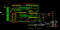
|
|
|
|
|
|
|
| Would any of the ICs be able to be replaced with more modern and smaller form factor? It would be cool to be able make something like a portable without it being too large | |
|
|
|
|
Last edited by L10N37 on Fri Sep 04, 2020 12:47 am; edited 1 time in total |
|
Yeah definitely. If you check Ali express someone in Asia completely re-engineered the VA4 megadrive mainboard. Although he spaced it out and it’s actually a lot bigger than the original lol. I don’t know enough about hardware to re-engineer the board it would take a lot of research, prototyping and trial and error. I’m still sweating it out about the output enable lines to the VRAM but they’d have to be pulsing at the same time. It hasn’t even being confirmed you can switch out the RAM to SRAM just in theory it should work. *sorry write enable
The only video I’ve seen on RAM replacements the guys switched out the ICs from donor boards I could be wasting my time but we will see, almost guaranteed my first board won’t work |
|
|
|
|
|
|
|
Also a good thing to consider is the megadrive / genesis V3 being the smallest form and having backwards compatibility with the SMS
Also the Gamegear which is already a handheld and runs sms games |
|
|
|
|
|
|
|
getting there
Looking over another schematic sheet, shows audio signal being pulled down with 2k2, a 180pf bypass cap for what ever reason and a 1uf ac coupling. Then another 10pf on the output before the 8 pin DIN I’ve used both audio input and output on my mods and it didn’t make a difference Modded by Bacteria grabs his audio straight off the VDP pin so I’m guessing the caps aren’t needed and only the pull down would come into effect. Not sure what the hell is going on with the C sync (looks like a bunch of gates), will need further investigation. I spoke to someone on another thread on here about it and he mentioned a single pull up resistor on the model 2’s and just needing to pull the TTL down with a resistor and the ac coupling cap ... will check some other sheets tomorrow This sheet has the c sync out not even connected , which is where I grab sync for my modded model 2’s and these come out pretty much bang on... Ready to use. Pretty sure I checked it with a little baby oscilloscope and it was all G I just passed it thru 75ohms **actually I can see the 2k2 pull-up, I think the rest of just to mix it with composite thru the Sony IC *ugh followed labels and jumped layers on one of the pause gates pins when they can be swapped 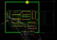
|
|
|
|
|
|
|
Sort of. The VA1 revision of the Genesis 3 is the only one that has backwards compatibility, and even then it needs to be modified. The VA2 revision of the Gen 3 (most common one I've come across) doesn't have any compatibility with the SMS. |
|
|
|
|
|
|
ah ok, didn't know that |
|
|
|
|
|
|
|
Refresh tighed high on VRAM causing auto labeling Z80 and cart connectors refresh to +5v
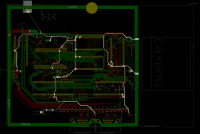
separated refresh labeling from Z80 to cartridge, ran missing refresh track from CPU to Cart connector Power supply will be something like this http://www.electronicecircuits.com/electronic-circuits/7805-5v-1a-regulated-powe... "It is an electrical circuit used to prevent an overvoltage condition of a power supply unit from damaging the circuits attached to the power supply. If the voltage regulator (7805) is faulty, the supply voltage could be applied to the load and it will damage our sensitive circuits. So we need this type of protection circuit. " substituting the 7805 with LM2940CT + 220uf cap to set output at +5v created footprint for AV out header. finished controller stuff, still may add a jumper on VCC to disable/ enable the pause. Need to measure out pause button. If it doesn't fit it will be left off. re-arranging at this stage is a major pain in the A. Placed all components, routed power and ground tracks, added optional LED footprint/ resistor. Not much left to go until final tidy up and checks. Will make a checklist of each pin for each IC, and basically check everything off eventually *MISSED p1 ground for controller input. I still find it weird this passes through an EMI filter to ground, essentially leaving all 3 pins to ground.. but the input ground separate from the entire boards earth plane... should be right... i think *moved din connector across, should be to centre not to edge of connector 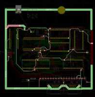
|
|
|
|
|
|
|
| Looking good. Have you thought about adding in 3D glasses support? The circuit isn't too complicated https://circuit-board.de/forum/index.php/Thread/26728-TUT-3D-Support-f%C3%BCr-da... but might be a pain to add in now that you have done some routing already. | |
|
|
|
|
|
Looks like this blokes got it covered... I wonder what 3D glasses that come with televisions would do on those games? I had a Sharp Aquos that came with a pair of Gimicky glasses :P |
|
|
|
|
|
|
|
This is what I've come up with for the PSU using the link above as a guide.
Went too hard on the drinks lastnight, so won't go much further today. Needs labelling, footprints and so forth before I place it. need to find a switch which matches close enough to the original... shouldn't be too hard but a quick browse looks like the slide notch is a bit too wide on most. POWER SUPPLY PWR_JACK 694108301002 PWR_SW SCR1 2P4M ebay F1 1a fuse 1206 0466001.NR. R9 330Ω ¼W MCMF0W4FF3300A50 R10 33Ω ¼W MCMF0W4FF330JA50 C22 100µF 50V 50YXF100MEFC8X11.5 C23 22uf-470uf 50v/63v LOW ESR C24 0.1uf tantalum MCCB1V104M2ACB or ceramic: MCMLR50V104KX7R C25 0.47µF tantalum MCCB1V474M2ACB/ 199D474X0035A1V1E3/ MCDTR47M35-1-RH C26 0.1uf film B32529C1104J189/ ECQE2104JF D2 1N4001 D3 1N4001 D4 6.2V Zener Diode ¼W BZX84-C6V2,215 LM LM2940CT A/V OUTPUT 8P_DIN 671-0801 (C-type) https://imgur.com/6yjyhZl 
mistakes or suggestion let me know. This will be going back to a standard centre positive like normal people use everyday. At the moment i prefer to use aftermarket supplies anyway, and need to run them through polarity switches (little section of cable) 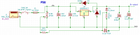
|
|
|
|
|
|
|
|
I wouldnt bother with the over voltage protection. Unless you invisage the regulator failing then its probably not needed. As long as its not over loaded and its properly heat sinked you shouldnt have any issues.
If you want to be cleaver id put a bridge rectifier between the power socket and the regulator. Then the polarity of the power adapter can be either way around and you also dont have to worry about reverse polarity protection. Youll have a bit of voltage drop across the bridge rectifier but with using the ldo regulator youll still be fine with a 9v power adapter. |
|
|
|
|
|
|
|
its cos the LM2940 is dependent on the output cap to actually output 5v... so if that cap fails or deteriorates badly you would overload every IC on the board. It's a bit of extra protection in case I've made any mistakes so i don't fry every IC on the board.
I know what you're saying, it seems a little overboard considering these old consoles almost never fail.. and if the regulator fails it only ever needs replacing. They're also protected from reverse polarity from factory. I was just going to lay a bare patch of copper and a mounting hole to tie down the regulator and use the PCB as a heatsink |
|
|
|
|
|
|
|
It's odd that your PSU protects from lots of weirdly rare issues, but doesn't even protect input capacitors from reverse polarity.
1n400x diode (reverse polarity protection) -> 470µF (filtering) -> pre LDO capacitor -> LDO -> post LDO capacitor -> done. |
|
|
|
|
|
Last edited by L10N37 on Mon Sep 07, 2020 3:09 pm; edited 4 times in total |
|
It’s not mine, I just took off the LED part of the schematic off it (LED/ resistor) and adjusted the smaller input cap to the one off the Regulators data sheet. I adjusted the small output cap to one off the original master system supply schematic. The output minimum is 22uf and is necessary To set 5v output . Original plan had 10uf. These need minimum 22uf or they don’t output 5v hence wanting over voltage protection as the entire system running on 5v is dependant on that output capacitor (C23). It also does provide reverse polarity protection
I was able to run my megadrive V1 off 6v input with a pair of these regulators :) 
forgot to move the ground, but same thing 
|
|
|
|
|
|
|
| Ultimately I could stick one diode on It and one big cap and run it off a 5v dc pack :p | |
|
|
|
|
|
|
I am going to look into another design using MIC2940 at some stage , no rush.
This crowbar design is a little heavy on components when it can be replaced with a $3.50 regulator that has built in protection from reverse polarity etc , can do away with the diode across input and output for reverse discharge and the other one providing the short should polarity be switched . That way we could also get rid of the fuse. |
|
|
|
|
|
|
|
Here’s a little demo of a cheap LDO regulator and why I don’t want to skimp on the power supply circuit . He wired this bare bones as per schematic provided The factory sega packs are rated at 9 or 10v mine does just off 14v with no load and we have everdrive circuit pulling extra ma |
|
|
|
|
|
|
|
The use of ferrite beads for frequency filtering on the master systems.
The Taiyo yuden ones used (FBA04VA600VB) are discontinued. should be able to use BL01RN1A1D2B in replacement. Will decide on the Power supply circuit soon They're also on the clock line to the Z80 there (FBR07HA121SB-00) 
|
|
|
|
|
|
|
| I seem to remember that Everdrive can be harmful because it lacks the correct level shifters (?), so if you’re embedding one you might consider adding those. | |
|
|
|
|
|
This was in 2017 i think something about a dodgy way they step down the 5v for the 3.3v circuitry in the everdrive 
I've decided on this, that regulator should offer the same protection as the diode. Nice and simple. Won't be updates for a long time... until the board and IC's arrive and it's assembled and tested :) Project almost over 
|
|
|
|
|
|
|
| Youd still want a diode to protect the pre regulator caps from reverse polarity. | |
|
|
|
|
|
Cheers wasup, thought to throw one on then thought ah nah the regulator does the job. Didn’t think ah yeah they form a link across the rails , backwards in polarity hahaha If anyone’s interested in these adapters hit me up, it was just for fun to reverse engineer one with a multimeter and now have to get rid of a bunch due to MOQ. 100% compatible. Works with everdrive too. No creds for engineering this it’s an analogue SG adapter clone https://imgur.com/gallery/lWqPwUW |
|
|
|
|
|
|
|
that's only 100% compatible with SMS library via everdrive. I found Raphnet who had already made an adapter and provided a lot of information.
Anyway that's off topic. I will make some adjustments to the PSU and stuff and finish the board and post some pics before I order a proto the input cap isn't what's recommended on the datasheet. Think i found a winner for the switch, would prefer a little higher rating consoles rated at 500ma switch at 600ma but i doubt it's going to pull close to that STSSS9221 |
|
|
|
|
|
|
|
OK, im over schematic labelling and bla bla
this is "off sheet" stuff quick dirty throw together. all that should be left is solder pads for RGB for bypass board, external video circuit Sync will go straight to sync pin with 2k2 pullup, 470ohm resistor Audio needs pulldown resistor , straight to audio pin. It's a C type 8 Pin DIN out which you can easily get scart cables for. Mine are all V pin and i accidentally ordered a C at some stage so have a spare. 

Obviously board needs a massive tidy up, and zones filled with ground, and labels all moved around for components and tidied up so it's neat ** and some mounting holes which might screw things up 
|
|
|
|
|
|
|
|
quick pre-clean up and check preview
Audio 2k2 pull down 180pf bypass 1uf ac couple to pin 1 C-Sync 2k2 pull up, 470ohm resistor in series to pin 3 solder enable pause hack, disconnects the norgate added solder pads for RGBs/5v/gnd input and output added 

*forgot c sync out capacitor *final today up later and order Hopefully with lower voltage input the regulator doesn’t get *too* warm. The heatsinks for these are pretty big 
|
|
|
|
|
Goto page 1, 2 Next |