|
|
DevelopmentSega Master System / Mark III / Game Gear |
Home - Forums - Games - Scans - Maps - Cheats - Credits |
SMS Official Docs
Software Reference Manual for the SEGA Mark III Console
- The Sega Mark III Game Console
- THE CPU
- THE VIDEO DISPLAY PROCESSOR (VDP)
- MEMORY MANAGEMENT
- INPUT/OUTPUT (I/O) PORTS
- PROGRAMMABLE SOUND GENERATOR (PSG)
- Appendix A - VDP Registers
- APPENDIX B - INPUT/OUTPUT SYSTEM
- Appendix C
- Appendix D
The Sega Mark III Game Console
This manual describes the SEGA Mark III game console hardware. The manual is divided into five sections:
The CPU.
The Video Display Processor (VDP).
The Memory Management System.
The Input/Output System.
The Programmable Sound Generator (PSG).
Each section begins with a general description, followed by a detailed description of every control bit. Several pictorial diagrams at the back of the manual tie together all of the concepts described in the manual. If you wish to see how a particular feature fits into the total system, refer to these back pages
HEADINGS
Important topics inside each section is marked as above with a "heading". This allows quick scanning for specific items of interest.
FORWARD REFERENCES
In some sections it is impossible to describe the system without making references to technical details described further forward in the manual. For example you will find reference to "Sprite Interrupts" in the CPU section, before the notion of a sprite is discussed in the VDP section.
For this reason you might find it helpful to browse the first parts of each section to get a feel for the total system before diving into the detailed descriptions.
The system will hereafter be referred to as the "Mk3".
THE CPU
The Mk3 uses a Z80A microprocessor, clocked at 3.58 MHz.
The implementation of Z80 features as they pertain to the Mk3 are described in this section.
RESET
The Z80A executes a RESET cycle when the base unit is turned on. This is the only Z80A reset mechanism implemented.
The momentary RESET button on the console does not control Z80A reset; it is attached to an input port for software polling.
INTERRUPT SYSTEM
The Mk3 implements two of the Z80 interrupts, the Non-maskable Interrupt (NMI), and the Maskable Interrupt (INT).
NMI
The NMI pin is connected to the console "PAUSE" button. Pressing this button causes the Z80 to execute a Restart instruction at location $66. This acts as a simple subroutine call: the PC is pushed onto the stack and a jump to $0066 is performed.
This interrupt is "edge-triggered", which means that if the PAUSE button is held down, you will get a single interrupt only.
NOTE: The last instruction of your NMI routine must be "RETN", Return from Non-Maskable Interrupt.
The PAUSE button is for the exclusive use of your program; you must set up the transfer of control at $0066 to your PAUSE routine.
The most common PAUSE routine will toggle a software "pause" flag and turn off the sounds if this flag has just been set. The INT routine, which is periodically activated, then checks the condition of the pause flag and does no processing if it is set (it loops on the pause flag).
This method allows the pause feature to be implemented without turning the interrupts off and on (with a DI and later an EI instruction). This DI-EI combination can cause a spurious interrupt in the Z80.
The NMI cannot be inhibited.
INT
This interrupt is enabled with an "EI" instruction, and disabled with a "DI" instruction.
The Mk3 hardware supports the "mode 1" interrupt only. The boot ROM executes the "IM 1" instruction at power-on.
In mode 1, activating the Z80A INT pin causes a Restart instruction to be executed at location $38 if interrupts are enabled.
This interrupt can be activated by two events in the VDP chip:
1. Vertical Blanking Interval.
2. Horizontal Line Counter.
Here is a skeleton program for an Interrupt response routine:
(at $0038)
.
.
INT PUSH AF
IN A,(0BFH)
.
.
.
POP AF
EI
RET
The first step is to save the working registers and flags. Other "PUSH" instructions should be added for any registers your interrupt routine will use.
Reading the I/O part at $BF does two things. First, it clears the interrupt request line from the VDP chip. Second, it provides VDP information as follows:
bit 7 — 1: VBLANK Interrupt, 0: H-Line Interrupt [if enabled].
bit 6 — 1: 9 sprites on a raster line.
bit 5 — 1: Sprite Collision.
bits 4-0 (no significance).
The VDP VBLANK and H-Line interrupts are enabled with the IE and IE1 bits in VDP registers 0 and 1, as shown in the following chart:
Interrupt Enable Bits
| IE (R1 bit 5) | IE1 (R0 bit 4) | Interrupt Source |
|---|---|---|
| 0 | 1 | H-Line Interrupt only. |
| 1 | 1 | Both H-Line and VBLANK. |
When an INT is accepted, the interrupt system is turned off, exactly as if a "DI" instruction had been executed. Thus, the code to exit from an interrupt routine should restore the registers, execute an "EI" instruction, and return.

THE VIDEO DISPLAY PROCESSOR (VDP)
The Mk3 uses an advanced video controller chip called the VDP (Video Display Processor). The VDP is a Sega designed custom chip whose architecture resembles an enhanced TMS9918A.
The screen resolution of the VDP is 256 pixels horizontal, and 192 pixels vertical. A pixel can be shown as one of sixteen colors, selected from a palette of 64 different colors.
16 Kilobytes of RAM are dedicated to the video system. This RAM (called the video RAM) is attached directly to the VDP chip, and does not appear in the Z80 memory space. The Z80 reads and writes the Video RAM through VDP registers.
The VDP implements two independent graphic systems, a background system and a sprite system.
VIDEO RAM ORGANIZATION
The 16 Kilobyte Video RAM is divided into three sections:
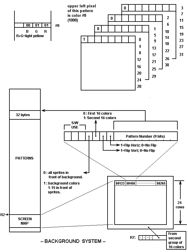
1. A 1792 byte screen map. This map determines the placement of character cells (sometimes known as "tiles") on the background screen's 32 by 24 grid.
2. A 256 byte sprite attribute table. This table sets the X-Y coordinates and character number of up to 64 moveable objects, or sprites.
3. A 14,336 byte character generator. These are 8 by 8 pixel character patterns for the background, and/or 8(h) by 8(v) or 8(h) by 16(v) pixel character patterns for the sprites.
32 bytes define a single 8 by 8 pixel character. The character generator portion of the Video RAM thus is capable of defining up to 448 characters.
The placement of the three Video RAM sections is controlled by registers in the VDP. As we'll see, you have some choice over where they appear in the 16K Video RAM memory map.
COLOR
The attribute of color is carried in the character patterns in the character generator portion of the Video RAM. Each pixel in the character pattern contains 4 bits of information. A choice of sixteen colors is thus available for every pixel.
The sixteen available colors are not fixed. they are stored in a Color RAM inside the VDP chip. The Color RAM is organizeed as 32 6-bit values. The six bits provide four levels (2 bits) of red, green, and blue.
Note that 32 color values represent twice the addressing capability of the 4-bit pixels. Other VDP control bits allow selection of the 16 value color table from either the first half or the second half of the Color RAM.
BACKGROUND SYSTEM
The background system is composed of "characters" which are eight pixels high and eight pixels wide. The screen is organized as 768 visible characters: 32 horizontal by 24 vertical.
An additional 4 character rows exist below the 24 visible vertical rows. These additional rows are useful for scrolling new background information upwards onto the screen.
2048 bytes of the video RAM function as the screen map. This map defines the screen positions of 896 characters (768 visible).
At every character position, there is a 16-bit (2 byte) word which describes the following:
- Which of 512 characters to display at the character position (9 bits).
- Whether or not to flip the character horizontally or vertically (2 bits).
- Which of two sets of 16 colors to use for the character (1 bit).
- Whether sprites obscure the background, or vice versa (1 bit).
- Three uncommitted bits, useful for software flags (3 bits).
The visible screen map occupies 1536 bytes of video RAM (768 characters, two bytes per character).
The nonvisible four rows of characters below the visible screen occupy 256 bytes (128 characters, two bytes per character).
This leaves 256 bytes of unused memory at the highest address of the 2048 byte screen map RAM. These 256 bytes are normally used to store the Sprite Attribute Table.
This memory could also be used to store eight character patterns, if the Sprite Attribute Table is located elsewhere. If the screen map is placed at $3800 (the usual case), the character numbers for the unused 256 bytes of screen map RAM are $1F0 through $1F7.
SCROLL INHIBIT BITS
The background screen can be scrolled in one pixel increments both horizontally and vertically. Two "scroll inhibit" bits allow you to inhibit scrolling in two screen areas:
If HSI (Horiz Scroll Inhibit) is set to 1, the 2 character high horizontal strip at the top of the screen does not scroll.
If VSI (Vert. Scroll Inhibit) is set to 1, the vertical band of 8 characters at the right edge of the screen does not scroll.
This feature simplifies the placement of score information at the top or right side of the screen. When the background screen playfield scrolls, the scores remain in place if the scroll inhibit bits have been set.
SPRITES
A sprite is an easily movable object. The VDP provides 64 independent sprites. A control bit controls the size of all sprites: 0 for an 8H by 8V spite, 1 for an 8H by 16V sprite.
Each sprite uses a three byte entry in a Sprite Attribute Table (in Video RAM) to set it's vertical and Horizontal position, and to select one of 256 characters to be displayed for the sprite.
A VDP control bit (Sprite Shift, bit 3 of R0) shifts all sprites 8 pixels to the left. This allows sprites to smoothly scroll off the left edge of the screen.
Sprite and background characters are drawn from the same "pool" of character patterns in video RAM. Thus sprites have the same color capabilities as background characters: 16 colors at a time from a choice of 64 colors.
Sprite colors are always taken from the second group of 16 colors in the color RAM.
Sprites do not scroll when the background scene is scrolled.
Sprites can be placed over or under other sprites. Sprites can also appear over or under characters in the background scene.
Up to eight sprites can occupy a single horizontal raster line. A VDP status register bit is provided to alert you when nine or more sprites are positioned on the same line. A horizontal raster line containing nine or more sprites is not displayed properly.
Another VDP status register bit indicates that two sprite patterns touched (collided).
SPRITE ATTRIBUTE TABLE
A 256 byte section of Video RAM functions as the Sprite Attribute Table. VDP register R5 is usually set to $FF to position the Sprite Attribute Table at $3F00, the last 256 bytes of Video RAM.
The Sprite Attribute Table is organized as shown on the table on the next page.
Sprite Attribute Table Organization
| Address | Attribute |
|---|---|
| 3F00 | vpos #0 |
| 3F01 | vpos #1 |
| 3F02 | vpos #2 |
| 3F03 | vpos #3 |
| 3F04 | vpos #4 |
| 3F05 | vpos #5 |
| 3F06 | vpos #6 |
| 3F07 | $D0 (terminator) |
| ... | |
| 3F3E | |
| 3F3F | vpos #63 |
| 3F40..3F7F | 64 unused bytes. [Can put two 32 byte character patterns here and address as char's $1FA and $1FB]. |
| 3F80 | hpos #0 |
| 3F81 | char code #0 |
| 3F82 | hpos #1 |
| 3F83 | char code #1 |
| 3F84 | hpos #2 |
| 3F85 | char code #2 |
| 3F86 | |
| 3F87 | |
| ... | |
| 3FFE | hpos #63 |
| 3FFF | char code #63 |
The special code $D0 is placed as a vertical position code to tell the sprite hardware to stop searching the list for sprites. All sprites which occur after the $D0 entry are disabled.
When two sprites overlap, the higher numbered sprite will be displayed on top. The overlap priority is thus set by the positions of the sprites in the table.
The horizontal position bytes locate the upper left corner of the sprite at one of 255 horizontal coordinates on the screen. An hpos=0 puts the sprite on the left column of the screen (left 8 pixels). An hpos=255 puts the sprite at the last pixel column; only the left column pixels of the sprite are seen and the other 7 columns in the sprite pattern are blanked.
This makes it easy to smoothly scroll a sprite off the right edge of the screen.
Setting a VDP Sprite Shift bit (R0, bit 3) shifts all sprite patterns eight pixels to the left. This allows sprites to be smoothly scrolled off the left edge of the screen.
If smooth appearing and disappearing of sprites is desired on both edges of the screen, another VDP control bit (R0, bit 5) can be set to 1 to blank the left column of characters.
Thus if R0 bit 3 is set to 0 (no shift left), and R0 bit 5 is set to 1 (blank left column), the screen is reduced to 31 character columns, and sprites enter and leave the screen smoothly. The left edge is handled by the fact that sprite hpos=0 puts the sprite in the left column, which is blanked in this mode.
SPRITE/BACKGROUND DISPLAY PRIORITY
Sprites can appear in front of or behind the background scene. This is controlled by bit 12 of the 16-bit background character code. If this bit is set to 0, all sprites appear over the background. If this bit is set to 1, background colors #1-15 appear over the sprites. Background color #0 always appears under the sprites.
COLOR RAM
The VDP chip contains a color RAM of 32 6-bit values. These values are formatted as "write only" 8-bit bytes:
| X | X | B1 | B0 | G1 | G0 | R1 | R0 |
where R1:R0, G1:G0 and B1:B0 define four intensities for red, green, and blue as follows:
| R,G,B-1 | R,G,B-0 | Intensity |
|---|---|---|
| 0 | 0 | Off |
| 0 | 1 | 1/3 |
| 1 | 0 | 2/3 |
| 1 | 1 | 3/3 (brightest) |
The color RAM is organized as two banks of 16 colors each. Colors are selected from either bank with a four bit color code.
CHARACTER PATTERNS
The actual dot patterns for screen images are called characters. Character patterns are used by both the background system and the sprites.
Every character is made up of 32 bytes. These bytes are orgaized as eight 4 byte groups, where each 4 byte group forms one row of pixels.
Four bits are required to select 16 colors. These bits come from corresponding bits in the four planes. The table on the next page shows a 32 byte character patern. "0's" are shown as periods for clarity.
AN EXAMPLE CHARACTER PATTERN
| Byte | b7 | b6 | b5 | b4 | b3 | b2 | b1 | b0 | ||
|---|---|---|---|---|---|---|---|---|---|---|
| 0 | 1 | 1 | 1 | 1 | 1 | 1 | 1 | 1 | c0 | FIRST PIXEL ROW '0101' = color #5 |
| 1 | . | . | . | . | . | . | . | . | c1 | |
| 2 | 1 | 1 | 1 | 1 | 1 | 1 | 1 | 1 | c2 | |
| 3 | . | . | . | . | . | . | . | . | c3 | |
| 4 | . | . | . | . | . | . | . | . | c0 | SECOND PIXEL ROW: '1100' = color #12, '0000' = color #0. |
| 5 | . | . | . | . | . | . | . | . | c1 | |
| 6 | 1 | 1 | . | . | . | . | . | . | c2 | |
| 7 | 1 | 1 | . | . | . | . | . | . | c3 | |
| 8 | . | . | . | . | . | . | . | . | c0 | THIRD PIXEL ROW |
| 9 | . | . | . | . | . | . | . | . | c1 | |
| 10 | 1 | 1 | . | . | . | . | . | . | c2 | |
| 11 | 1 | 1 | . | . | . | . | . | . | c3 | |
| 12 | . | . | . | . | . | . | . | . | c0 | FOURTH PIXEL ROW |
| 13 | . | . | . | . | . | . | . | . | c1 | |
| 14 | 1 | 1 | . | . | . | . | . | . | c2 | |
| 15 | 1 | 1 | . | . | . | . | . | . | c3 | |
| 16 | . | . | . | . | . | . | . | . | c0 | FIFTH PIXEL ROW |
| 17 | . | . | . | . | . | . | . | . | c1 | |
| 18 | 1 | 1 | . | . | . | . | . | . | c2 | |
| 19 | 1 | 1 | . | . | . | . | . | . | c3 | |
| 20 | . | . | . | . | . | . | . | . | c0 | SIXTH PIXEL ROW |
| 21 | . | . | . | . | . | . | . | . | c1 | |
| 22 | 1 | 1 | . | . | . | . | . | . | c2 | |
| 23 | 1 | 1 | . | . | . | . | . | . | c3 | |
| 24 | . | . | . | . | . | . | . | . | c0 | SEVENTH PIXEL ROW |
| 25 | . | . | . | . | . | . | . | . | c1 | |
| 26 | 1 | 1 | . | . | . | . | . | . | c2 | |
| 27 | 1 | 1 | . | . | . | . | . | . | c3 | |
| 28 | . | . | . | . | . | . | . | . | c0 | EIGHTH PIXEL ROW '0010' = color #2 |
| 29 | 1 | 1 | 1 | 1 | 1 | 1 | 1 | 1 | c1 | |
| 30 | . | . | . | . | . | . | . | . | c2 | |
| 31 | . | . | . | . | . | . | . | . | c3 | |
This pattern represents a multicolor letter "C".
The top section is color #5 (reading corresponding bits from MSB to LSB, 0101).
The vertical section is color #12 (1100).
The bottom section is color #2 (0010).
Which colors these represent depends on the values stored in color RAM locations 2, 5 and 12.
NOTE: the 8 by 8 character background color is #0 (0000).
VDP REGISTERS
The VDP is controlled by eleven internal 8-bit registers. This section describes the method by which the Z80A acesses these registers, and then discusses the function of the individual registers.
The Z80 "sees" the VDP chip through two I/O port locations, $BE and $BF. I/O location $BF is the COMMAND register for a write, and the STATUS register for a read.
I/O port $BE is the read/write DATA register.
The Command Register is written twice in succession for all command operations; the data register may be read or written any number of times in succession, depending on the operation.
Because the command register is sequence sensitive, requiring a pair of outout bytes per operation, a DI instrucion should precede command register updates. This prevents, for example, an interrupt service routine that reads the VDP status register from disrupting the two byte synchronization.
There is a timing constraint for accessing the VDP chip.
The VDP chip cannot process data any faster than the following rates:
- 16 Z80A T-States during VBLANK
- 29 Z80A T-States during active video.
This means that you should never issue two consecutive OUT or IN instructions to the VDP; they should be separated by at least a NOP instruction.
This constraint applies to Video RAM and Color RAM as well as the internal registers.
A two bit mode field in bits 7 and 6 of the second COMMAND byte determines one of four operations:
| b7 | b6 | Operation |
|---|---|---|
| 0 | 0 | Read 16 Kbyte VDP RAM |
| 0 | 1 | Write 16 Kbyte VDP RAM |
| 1 | 0 | Write VDP Register |
| 1 | 1 | Write Color RAM |
To set up for the first two operations, read/write Video RAM the two COMMAND bytes have the following format:
Read VDP RAM
| First byte written to $BF | A7 | A6 | A5 | A4 | A3 | A2 | A1 | A0 |
|---|---|---|---|---|---|---|---|---|
| Second byte writen to $BF | 0 | 0 | A13 | A12 | A11 | A10 | A9 | A8 |
Write VDP RAM
| First byte written to $BF | A7 | A6 | A5 | A4 | A3 | A2 | A1 | A0 |
|---|---|---|---|---|---|---|---|---|
| Second byte writen to $BF | 0 | 1 | A13 | A12 | A11 | A10 | A9 | A8 |
After the COMMAND bytes have been output, data can be read at Input Port $BE or written at Output Port $BE.
The VDP has an address auto-increment feature. Once the Video RAM starting address has been loaded, the data (I/O port $BE) may be repeatedly accessed, and the address will automatically increase by one byte for every access.
NOTE: The autoincrement feature works only with all reads or all writes. Changing from read to write or vice versa requires two writes to the command register to reselect the mode.
The COMMAND register format for writing a VDP register (they are write-only) is shown below:
Write VDP Register
| First byte written to $BF | A7 | A6 | A5 | A4 | A3 | A2 | A1 | A0 |
|---|---|---|---|---|---|---|---|---|
| Second byte writen to $BF | 1 | 0 | 0 | 0 | r3 | r2 | r1 | r0 |
The register number is r3-r0, and ranges from 0 through 10 ($00 through $0A). The data to be written to the register is d7-d0.
For the "write register" operation only, there is no write to the DATA register at $BE, since the data (d7-d0) is contained in the first byte of the COMMAND byte pair.
The final command mode allows writing color values to the write-only VDP Color RAM.
Write VDP Color RAM
| First byte written to $BF | 0 | 0 | 0 | A4 | A3 | A2 | A1 | A0 |
| Second byte writen to $BF | 1 | 1 | 0 | 0 | 0 | 0 | 0 | 0 |
After loading this pair of bytes to the COMMAND register, the color RAM data is written to Output Port $BE in the following format:
| Color RAM Data written to $BE | 0 | 0 | b1 | b0 | g1 | g0 | r1 | r0 |
|---|
Where b1-b0 set four intensities for blue, g1-g0 set four intensities for green, and r1-r0 set four intensities for red.
As with the Video RAM, repeated writes to Output Port $BE automatically increment the Color RAM address. Color RAM addresses are mapped as shown on the next page.
| Color RAM Address | Color Number |
|---|---|
| 00000 ($00) | Bank1, Color 0 |
| 00001 ($01) | Bank1, Color 1 |
| 00010 ($02) | Bank1, Color 2 |
| 00011 ($03) | Bank1, Color 3 |
| 00100 ($04) | Bank1, Color 4 |
| 00101 ($05) | Bank1, Color 5 |
| 00110 ($06) | Bank1, Color 6 |
| 00111 ($07) | Bank1, Color 7 |
| 01000 ($08) | Bank1, Color 8 |
| 01001 ($09) | Bank1, Color 9 |
| 01010 ($0A) | Bank1, Color 10 |
| 01011 ($0B) | Bank1, Color 11 |
| 01100 ($0C) | Bank1, Color 12 |
| 01101 ($0D) | Bank1, Color 13 |
| 01110 ($0E) | Bank1, Color 14 |
| 01111 ($0F) | Bank1, Color 15 |
| 10000 ($10) | Bank2, Color 0 |
| 10001 ($11) | Bank2, Color 1 |
| 10010 ($12) | Bank2, Color 2 |
| 10011 ($13) | Bank2, Color 3 |
| 10100 ($14) | Bank2, Color 4 |
| 10101 ($15) | Bank2, Color 5 |
| 10110 ($16) | Bank2, Color 6 |
| 10111 ($17) | Bank2, Color 7 |
| 11000 ($18) | Bank2, Color 8 |
| 11001 ($19) | Bank2, Color 9 |
| 11010 ($1A) | Bank2, Color 10 |
| 11011 ($1B) | Bank2, Color 11 |
| 11100 ($1C) | Bank2, Color 12 |
| 11101 ($1D) | Bank2, Color 13 |
| 11110 ($1E) | Bank2, Color 14 |
| 11111 ($1F) | Bank2, Color 15 |
[Note: Background colors can be taken from either the first group of sixteen or the second group of sixteen colors. Border colors and sprite colors are taken from the second group of sixteen colors.]
The command register has one additional function. When it is read with an IN ($BF) instruction, it functions as an interupt status register, and also clears interrupt requests from the VDP chip.
VDP REGISTER UPDATES
In general, all VDP updates should be done while the TV's video signal is blanked. If operations that affect the screen appearance are not done during screen blanking, the screen will appear to have "noise" in the picture.
Your program can detect horizontal and vertical blanking intervals using the interrupt system and VDP flag bits. This capability is discussed in the CPU section.
It is not necessary to synchronize VDP initialization with blanking intervals, since the screen can be blanked prior to the setup operations, and then turned on when the initialization is complete.
VDP REGISTER DESCRIPTION
Register 0
Register 1
R0 and R1 set the VDP display and interrupt mode.
R0:
| b7 | VSI | Vertical Scroll Inhibit (right 8 char columns). 0: Scroll along with background. 1: Fixed (no scroll). |
|---|---|---|
| b6 | HSI | Horizontal Scroll Inhibit (top 2 char rows). 0: Scroll along with background. 1: Fixed (no scroll). |
| b5 | LCB | Left Column Blank. 0: Normal Display. 1: Blank left char column (border color). |
| b4 | IE1 | Interrupt Enable. |
| b3 | SS | Sprite Shift. 0: Normal sprite position. 1: Shift all sprites 8 pixels to the left. |
| b2 | 1 | [Always set this to 1]. |
| b1 | 1 | [Always set this to 1]. |
| b0 | ES | External Sync. [Always set this to 0]. |
R1:
| b7 | 1 | [Always set this to 1]. | |
|---|---|---|---|
| b6 | DIS | Display ON. 0: Blank whole screen. 1: Normal video. | |
| b5 | IE | Interrupt Enable. | |
| b4 | 0 | [Always set this to 0]. | |
| b3 | 0 | [Always set this to 0]. | |
| b2 | 0 | [Always set this to 0]. | |
| b1 | SZ | Sprite Size. 0: All sprites are 8 by 8. 1: All sprites are 8 by 16. | |
| b0 | 0 | [Always set this to 0]. | |
The two bit interrupt control field is defined as follows:
| IE | IE1 | Enabled Interrupt: |
|---|---|---|
| 0 | 1 | Raster Line. |
| 1 | 1 | VBLANK and Raster Line. |
Register 2
R2 sets the base address for the screen map. It positions the 2048 screen map to one of eight starting addresses, on 2048 byte boundaries, according to the following table:
| R2 Value | Screen Map Base Address |
|---|---|
| $FF | $3800 <--- Normal Setting |
| $FD | $3000 |
| $FB | $2800 |
| $F9 | $2000 |
| $F7 | $1800 |
| $F5 | $1000 |
| $F3 | $0800 |
| $F1 | $0000 |
The normal setting for R2 is $FF, which positions the base address at $3800, the highest-addressed 2 KByte section of the 16 KByte Video RAM.
Register 3
R3 should always be set to $FF.
Register 4
R4 should always be set to $FF.
Register 5
R5 controls the base address for the Sprite Attribute Table. This 256 byte table can be positioned at one of 64 starting addresses in Video RAM.
The base address is formatted in R5 as follows:
| R5: | 1 | A13 | A12 | A11 | A10 | A9 | A8 | 1 |
|---|
The normal setting for R5 is $FF, which positions the Sprite Attribute Table at $3F00. When R2 is $FF, placing the screen map at $3800, and R5 is $FF, the unused top 256 bytes of screen map memory is occupied by the 256 byte Sprite Attribute Table.
Register 6
R6 sets the base address for the sprite patterns. Only two values are valid for R6:
| R6 Value | Sprite Patterns |
|---|---|
| $FB | First 8K of Video RAM <--- Normal Value |
| $FF | Second 8K of Video RAM |
The preferred location for the sprite patterns is in the first 8K of video RAM, since the full 8192 bytes are available for patterns. In the second 8K, 2048 bytes are lost to the screen map and Sprite Attribute Table. Thus 256 sprite patterns can be stored in the first 8K, but only 192 sprite patterns can be stored in the second 8K.
Register 7
R7 sets the border color. The border color is taken from the second bank of colors in VDP Color RAM.
| R7: | 1 | 1 | 1 | 1 | C3 | C2 | C1 | C0 |
|---|
Register 8
R8 sets the horizontal scroll value for the background scene. A value of $00 produces no scrolling. A value of $01 moves the background scene one pixel to the left, and moves the leftmost column of pixels to the rightmost column (the scrolling "wraps around").
Higher value of R8 "rotate" the screen horizontally to a maximum of 255 pixels for a value of $FF. Note that horizontal scrolling resembles a rotating vertical cylinder, with graphic information disappearing from the left side of the screen and reappearing on the right side of the screen.
Register 9
R9 sets the vertical scroll value for the background scene. A value of $00 produces no scrolling. A value of $01 moves the background scene one pixel upward. The vertical scrolling resembles a rotating horizontal cylinder, but the "wrap around" point is not at the screen edge, as with horizontal acrolling. Rather, it is at the 28th character row. (Remember that the screen is organized as 28 character rows, with the top 24 displayed on the screen).
Register 9 is latched in vertical blanking.
Register 10
R10 controls the Raster Line Interrupt.
The TV beam sweeps out horizontal lines (called raster lines) from left to right, moving from the top to the bottom of the screen. The visible picture contains 192 of these raster lines.
At the end of each raster line there is a brief blanking interval (HBLANK) in which the TV beam is turned off as the beam retraces from the right side to the left side of the screen. This HBLANK interval last approximately 10 microseconds.
It is desireable to receive an interrupt just after a selected raster line has been displayed. For example, you might want to change a color value after the beam has swept out the top half of the screen. In this case you would want to know when the 95th raster line has completed.
R10 allows you to do this. If you load R10 with 94, a Raster Line Interrupt Request will be generated every time the 95th horizontal line finishes it's scan.
The value loaded into R10 should be one less than the raster line you wish to "trigger" the interrupt.
The Raster Line Interrupt continues to generate interrupt requests as the beam sweeps the screen. The table on the next page shows the settings of R10 and the raster lines that generate interrupt requests at HBLANK time:
| R10 Value | Interrupt Requests at these HBLANK times |
|---|---|
| $C0-$FF | None |
| $00 | 1,2,3,4,5,...191 |
| $01 | 2,4,6,8,10,..190 |
| $02 | 3,6,9,12,....189 |
| $03 | 4,8,12,16,...188 |
| (etc) | (etc) |
There are two special cases: $FF turns off the interrupt requests, and $00 gives a Raster Line interrupt request for every horizontal line.
There is a one interrupt delay between loading R10 and having the value take effect. For example, if you set R10 for line 20, and respond to the interrupt by resetting R10 to 150, the very next Raster Line Interrupt will occur at 20, and all subsequent ones will occur at 150.
The VDP registers are initialized at power on to the following values:
| R0 | $36 | mode |
|---|---|---|
| R1 | $A0 | mode |
| R2 | $FF | Screen Map Table Base |
| R3 | $FF | (Always $FF) |
| R4 | $FF | (Always $FF) |
| R5 | $FF | Sprite Table Base |
| R6 | $FB | Sprite Pattern Table Base |
| R7 | $00 | Border color #0 |
| R8 | $00 | Scroll-H |
| R9 | $00 | Scroll-V |
| R10 | $FF | H-line interrupt ($FF=OFF) |
MEMORY MANAGEMENT
The Mk3 base unit contains 8 kilobytes of ROM and 8 Kilobytes of RAM. Game program ROM is plugged into the unit by using one of two slots.
The front slot accepts a slim cartridge that resembles a credit card. The present capacity of this card is 32 Kilobytes. A 128 Kilobyte card is in the works.
The top slot accepts a more conventional plastic-cased game cartridge. 128 Kilobyte cartridges are now in production. 256 Kilobyte and larger cartridges are in the works.
The Z80A processor is capable of addressing 64 kilobytes of memory. Because the added game cartridge memoy can exceed 64 Kilobytes, a simple memory management system is implemented in the Mk3.
When the Mk3 is turned on, the memory map contains an 8 kilobyte ROM at $0000, and an 8 Kilobyte RAM at $C000.
SYSTEM RAM
The RAM is mapped into two places, $C000-$DFFF and $E000-$FFFF. This RAM is used for Z80A stack and scratchpad use.
The top eight locations of RAM are reserved for memory management control registers, and should not be used by a game program.
For future compatibility, the RAM should be addressed at $C000-$DFFF. The stack should be placed at $DFF8.
MEMORY ENABLES
Output port $3E controls the memory enables. Individual bits in this port enable the System ROM, System RAM, Card Slot, Cartridge Slot, and External Slot. (The external Slot is not presently used).
Output port $3E has the following format:
OUT ($3E):
| bit 0 | don't care |
|---|---|
| bit 1 | don't care |
| bit 2 | 0: enable joysticks |
| 1: disable joysticks | |
| bit 3 | 0: enable base unit 8K ROM |
| 1: disable base unit 8K ROM | |
| bit 4 | 0: enable internal 8K RAM |
| 1: disable internal 8K RAM | |
| bit 5 | 0: enable card ROM |
| 1: disable card ROM | |
| bit 6 | 0: enable cartridge ROM |
| 1: disable cartridge ROM | |
| bit 7 | 0: enable external port |
| 1: disable external port |
MEMORY SELECTION AT POWER-ON
When the system is turned on, the Z80A begins executing code at location $0000 in the resident 8 Kilobyte ROM. This ROM code performs the following steps:
- The system is initialized.
- A small program is copied from ROM into the RAM (at $C700).
- The program jumps to $C700 to execute this prgram.
- All of the system ROM spaces are disabled. This is why the program is copied to RAM and run there--the ROM spaces can then be checked one by one.
- The ROM spaces are individually enabled and checked for the presence of memory. They are checked in the following order:
- Front card slot.
- Top cartridge slot.
- External (rear) slot.
- If memory is detected in any of these three slots, the slot is enabled and the Z80A executes a jump to location $0000.
- If no memory is detected, the console ROM is eneabled and an "Insert a cartridge" message is put on the screen.
Notice that if both the card and cartridge are plugged in, the card will be enabled because it is checked first.
A game program is written as a completely self-contained Z80A application program with origin $0000. A game program must take care of all system "housekeeping", for example setting up the interrupt vectors.
Once a game is running, there is no access to the boot ROM.
MEMORY MAPS
The following figures show memory maps for two presently defined memory sizes: 32 Kilobytes, and 128 Kilobytes.

Figure M-1 shows the Z80A memory map at power-on.
32 KILOBYTES
Figure M-2 shows the Z80A memory map for the 32 Kilobyte card. This is the simplest case: 32 Kilobytes starting at location $0000.
128 KILOBYTES
Figure M-3 shows the memory map for a 128 Kilobyte cartridge. (This is refered to in the Sega literature as a "Mega"(bit) cartridge).
As with the 32 KByte memory, there is a contiguous section of ROM in the bottom half of Z80A memory. This section is always available to the Z80A.
Additionally, there are six banks of 16 Kilobyte ROM at memory addresses $8000-$BFFF. Only one of these banks is available to the Z80A at a time. Whenever one is selected, the other five are inactive.
Which of the six banks is switched into the Z80A memory space is controlled by a register at memory location $FFFF.
The Bank Control Register has the following format:
| $FFFF | 0 | 0 | 0 | 0 | 0 | b2 | b1 | b0 |
|---|
The banks are numbered from 2 through 7 (b2:b1:b0).
Although this write-only register exists in the memory cartridge, writes to the register are duplicated in the RAM at $FFFF. This means that the bank select register appears to be read/write, even though what is actually read is the RAM image of the register, rather than the contents of the register itself.
THE CARTRIDGE HEADER
The presence of a cartridge is tested by checking for specific information in ROM. This information must be correct for the cartridge to be recognized.
Normally, Sega will add the correct information to the cartridge before production. The information below is given for reference only.
The header format is as follows (addresses shown for 32 KByte and larger cartridges):
At $7FF0:
The string, "TMR SEGA " [54,4D,52,20,53,45,47,41,20,20]
At $7FFA-$7FFB
A 16-bit checksum for the ROM (low-hi order). $7FFA and $7FFB are not included in this checksum.
At $7FFC-$7FFD
A 16-bit serial number, assigned by Sega.
At $7FFE
A software revision number byte.
At $7FFF
ROM Size code:
| $4A | 8K | (header at $1FF0) |
| $4B | 16K | (header at $3FF0) |
| $4C | 32K | |
| $4D | 48K | |
| $4E | 64K | |
| $4F | 128K | (1M) |
| $40 | 256K | (2M) |
INPUT/OUTPUT (I/O) PORTS
Eight I/O ports are used by the Mk3:
| Port | Direc | Function |
|---|---|---|
| $3E | out | Memory Enables |
| $3F | out | Joystick port control |
| $7E | in | Gun Spot (vertical) |
| $7F | in | Gun spot (horizontal) |
| out | Programmable Sound Generator (PSG) | |
| $BE | i/o | VDP Data Register |
| $BF | i/o | VDP Command/Status Register |
| $DC | in | Joystick port |
| $DD | in | Joystick port |
Port $3E is described in the MEMORY MANAGEMENT section.
Port $7F is described in the PSG section.
Ports $BE and $BF are described in the VDP section.
The remaining ports deal with the attached controls, and are described in this section.
Ports $DC-$DD are connected to the two 9-pin connectors on the front of the game console. Although these ports are called "joystick ports", there are actually three devices that can be plugged into the front connectors:
- The joystick controls which include a joystick and two push buttons.
- The gun.
- A "Sports Pad" that consists of a trackball and two push buttons.
The bits of input ports $DC and $DD are used for the joystick assembly, gun, and Sports Pad (Trackball). These two ports work in conjunction with port $3F, which sets the direction of four of the bits, and provides two strobe bits for the Sports Pad. The following table shows how the three ports are interpreted for the joystick and gun options. All bits shown are inputs.
| Port | Bit | Joystick | Gun |
|---|---|---|---|
| $DC | 0 | P1-up | --- |
| $DC | 1 | P1-down | --- |
| $DC | 2 | P1-left | --- |
| $DC | 3 | P1-right | --- |
| $DC | 4 | P1-SW1 | P1 Trigger |
| $DC | 5 | P1-SW2 | --- |
| $DC | 6 | P2-up | --- |
| $DC | 7 | P2-down | --- |
| $DD | 0 | P2-left | --- |
| $DD | 1 | P2-right | --- |
| $DD | 2 | P2-SW1 | P2 Trigger |
| $DD | 3 | P1-SW2 | --- |
| $DD | 4 | RESET* | RESET* |
| $DD | 5 | --- | --- |
| $DD | 6 | --- | P1 Light Pulse |
| $DD | 7 | --- | P2 Light Pulse |
| $3F | 0 | 1 | 1 |
| $3F | 1 | 1 | P1 Latch Enable |
| $3F | 2 | 1 | 1 |
| $3F | 3 | 1 | P2 Latch Enable |
| $3F | 4 | 1 | 1 |
| $3F | 5 | 1 | 1 |
| $3F | 6 | 1 | 1 |
| $3F | 7 | 1 | 1 |
HOW THE GUN WORKS
The gun contains a lens and photocell which "sees" a spot on the TV screen. This spot is circular, and increases in diameter as the gun's distance from the screen increases.
When the TV beam reaches the area at which the gun is pointed, two things happen:
- A negative pulse of approximately 20-30 microseconds is generated on port $DD bit 6 (Player 1) or port $DD bit 7 (Player 2). This pulse is wide enough to allow a software loop to recognize it. The width of this pulse will vary with the game setup and TV type.
- The beam position is latched into horizontal and vertical registers, which are read at input ports $7E (vertical) and $7F (horizontal).
The beam position can be latched either from a gun plugged into the player 1 connector, a gun plugged into the player 2 connector, or both. [NOTE: The player 1 connector is the left connector when the game console is viewed from the front].
Two bits in output port $3F determine which gun latches the beam position. These are shown as "P1 Latch Enable" and "P2 Latch Enable" in the preceding table.
The gun reading routine usually performs the following steps.
- The trigger switch is checked. Normally the gun is not checked until someone pulls the trigger. (Data is continuously available from the gun, however).
- When the trigger is pulled, wait for the next VBLANK.
- At VBLANK, put up an all white screen (all color bytes are $3F). This gives enough light intensity on the screen for the gun to read any position.
- During the next scan, continuously check the light pulse bit for a high to low transition. (P1 Light Pulse is at input port $DD bit 6; P2 Light Pulse is at input port $DD bit 7).
- When the pulse is detected, read the Horizontal Position Register at $7F and the Vertical position Register at $7E.
- Wait for a low to high transition on the Light Pulse bit. Then repeat step 5 for all active horizontal lines.
- When finished with one scan, restore the screen to the normal color values.
The gun responds to a circular spot on the TV, not a single pixel. As the circular spot is "seen" by the photocell in the gun, repeated negative pulses will occur on the Light Pulse bit for several consecutive horizontal scan lines.
The horizontal values of the detected circle will, as the vertical position register increments, decrease, increase, and then stop as the left edge of the scanned circle is read by the lens in the gun.
For this reason it is advisable to do some sort of averaging and extrapolation to arrive at a center position of the scanned circle.
HOW THE TRACKBALL WORKS
The interface to the trackball consists of six input bits and one output bit.
| Trackball | dir | Player 1 | Player 2 |
|---|---|---|---|
| b0 | in | $DC bit 0 | $DC bit 6 |
| b1 | in | $DC bit 1 | $DC bit 7 |
| b2 | in | $DC bit 2 | $DD bit 0 |
| b3 | in | $DC bit 3 | $DD bit 1 |
| S1 | in | $DC bit 4 | $DD bit 2 |
| S2 | in | $DC bit 5 | $DD bit 3 |
| STROBE | out | $3F bit 5 | $3F bit 7 |
Before using the trackball, the following two instructions should be executed to set the STROBE bit directions to output, and initialize the strobe signals to 1. NOTE: these instructions are executed in the power-on initialization.
OUT (03FH),A ; b5,b7 are actual strobe bit values
The strobe signal is then used to clock in four 4-bit nibbles b3-b0, which occur in the following order:
| Nibble # | Data | When STROBE is: |
|---|---|---|
| b3 b2 b1 b0 | ||
| 1 | X7 X6 X5 X4 | LO |
| 2 | X3 X2 X1 X0 | HI |
| 3 | Y7 Y6 Y5 Y4 | LO |
| 4 | Y3 Y2 Y1 Y0 | HI |
The X,Y positions of the trackball are represented as X7-X0 and Y7-Y0. These are 8-bit counters which wrap around from $FF to $00.
As the ball is spun to the right, the X value increase; as it is spun to the left, they decrease. As the ball is spun upward, the Y values increase; as it is spun downward, they decrease.
The timing of the STROBE transitions is important. Here is the required sequence:
Program Sequence to Read Trackball
[Start with STROBE HI].
- STROBE LO.
- Wait 80 microseconds.
- Read first nibble.
- STROBE HI.
- Wait 40 microseconds.
- Read second nibble.
- STROBE LO.
- Wait 40 microseconds.
- Read third nibble.
- STROBE HI.
- Wait 40 microseconds.
- Read fourth nibble.
- (done-STROBE is HI).
Appendix D shows working code to read the trackball each interrupt.
PROGRAMMABLE SOUND GENERATOR (PSG)
The PSG contains four sound channels, consisting of three tone generators and a noise generator. Each of the four channels has an independent volume control (attenuator). The PSG is controlled through output port $7F.
TONE GENERATOR FREQUENCY
The frequency (pitch) of a tone generator is set by a 10-bit value. This value is counted down until it reaches zero, at which time the tone output toggles and the 10-bit value is reloaded into the counter. Thus, higher 10-bit numbers produce lower frequencies.
To load a new frequency value into one of the tone generators, you write a pair of bytes to I/O locations $7F according to the following format:
| First Byte: | 1 | R2 | R1 | R0 | d3 | d2 | d1 | d0 |
|---|---|---|---|---|---|---|---|---|
| Second Byte: | 0 | 0 | d9 | d8 | d7 | d6 | d5 | d4 |
The R2:R1:R0 field selects the tone channel as follows:
| R2 | R1 | R0 | Tone Channel |
|---|---|---|---|
| 0 | 0 | 0 | #1 |
| 0 | 1 | 0 | #2 |
| 1 | 0 | 0 | #3 |
10-bit data is (msb) d9 d8 d7 d6 d5 d4 d3 d2 d1 d0 (lsb)
NOISE GENERATOR CONTROL
The noise generator uses three control bits to select the "character" of the noise sound. A bit called "FB" (Feedback) produces periodic noise or "white" noise:
| FB | Noise Type |
|---|---|
| 0 | Periodic (like low-frequency tone) |
| 1 | White (hiss) |
The frequency of the noise is selected by two bits NF1:NF0 according to the following table:
| NF1 | NF0 | Noise Generator Clock Source |
|---|---|---|
| 0 | 0 | Clock/2 [Higher pitch, "less coarse"] |
| 0 | 1 | Clock/4 |
| 1 | 0 | Clock/8 [Lower pitch, "more coarse"] |
| 1 | 1 | Tone Generator #3 |
Note: "Clock" is fixed in frequency. It is a crystal controlled oscillator signal connected to the PSG.
When NF1:NF0 is 11, Tone Generator #3 supplies the noise clock source. This allows the noise to be "swept" in frequency. This effect might be used for a jet engine runup, for example.
To load these noise generator control bits, write the following byte to I/O port $7F:
| Out ($7F): | 1 | 1 | 1 | 0 | 0 | FB | NF1 | NF0 |
|---|
ATTENUATORS
Four attenuators adjust the volume of the three tone generators and the noise channel. Four bits A3:A2:A1:A0 control the attenuation as follows:
| A3 | A2 | A1 | A0 | Attenuation |
|---|---|---|---|---|
| 0 | 0 | 0 | 0 | 0 db |
| 0 | 0 | 0 | 1 | 2 db |
| 0 | 0 | 1 | 0 | 4 db |
| 0 | 0 | 1 | 1 | 6 db |
| 0 | 1 | 0 | 0 | 8 db |
| 0 | 1 | 0 | 1 | 10 db |
| 0 | 1 | 1 | 0 | 12 db |
| 0 | 1 | 1 | 1 | 14 db |
| 1 | 0 | 0 | 0 | 16 db |
| 1 | 0 | 0 | 1 | 18 db |
| 1 | 0 | 1 | 0 | 20 db |
| 1 | 0 | 1 | 1 | 22 db |
| 1 | 1 | 0 | 0 | 24 db |
| 1 | 1 | 0 | 1 | 26 db |
| 1 | 1 | 1 | 0 | 28 db |
| 1 | 1 | 1 | 1 | -Off- |
NOTE: a higher attenuation results in a quieter sound.
The attenuators are set for the four channels by writing the following bytes to I/O location $7F:
| Tone Generator #1: | 1 | 0 | 0 | 1 | A3 | A2 | A1 | A0 |
|---|---|---|---|---|---|---|---|---|
| Tone Generator #2: | 1 | 0 | 1 | 1 | A3 | A2 | A1 | A0 |
| Tone Generator #3: | 1 | 1 | 0 | 1 | A3 | A2 | A1 | A0 |
| Noise Generator: | 1 | 1 | 1 | 1 | A3 | A2 | A1 | A0 |
EXAMPLE
When the Mk3 is powered on, the following code is executed:
LD C,PSG_PRT ; psg port is $7F
LD B,4 ; load four bytes
OTIR ; write them
(etc.)
CLRTB defb $9F,$BF,$DF,$FF
This code turns the four sound channels off. It's a good idea to also execute this code when the PAUSE button is pressed, so that the sound does not stay on continuously for the pause interval.
Appendix A - VDP Registers
| R0 | VScroll Inhibit | HScroll Inhibit | LEFT Col Blank | IE1 | Sprite Shift | 1 | 1 (M3) | 0 | |
|---|---|---|---|---|---|---|---|---|---|
| R1 | 1 | Screen Enable Bit | IE | 0 (M1) | 0 (M2) | 0 | Sprite Size 8/16 | Sprite Mag | |
| R2 | 1 | 1 | 1 | 1 | SCRN BASE 2 | SCRN BASE 1 | SCRN BASE 0 | $FF (Screen Base at $3800) | |
| R3 | 1 | 1 | 1 | 1 | 1 | 1 | 1 | 1 | $FF |
| R4 | 1 | 1 | 1 | 1 | 1 | 1 | 1 | 1 | $FF |
| R5 | 1 | SAT BASE 5 | SAT BASE 4 | SAT BASE 3 | SAT BASE 2 | SAT BASE 1 | SAT BASE 0 | 1 | $FF (SAT at $3F00) SAT = Sprite Attribute Table |
| R6 | 1 | 1 | 1 | 1 | 1 | CGEN BANK 0 | 1 | 1 | $FB (CGEN at $0000) CGEN = Character Generator |
| R7 | 1 | 1 | 1 | 1 | BORDER 3 | BORDER 2 | BORDER 1 | BORDER 0 | Border Color |
| R8 | HSCROLL 7 | HSCROLL 6 | HSCROLL 5 | HSCROLL 4 | HSCROLL 3 | HSCROLL 2 | HSCROLL 1 | HSCROLL 0 | $00 Horizontal Scroll <---- |
| R9 | VSCROLL 7 | VSCROLL 6 | VSCROLL 5 | VSCROLL 4 | VSCROLL 3 | VSCROLL 2 | VSCROLL 1 | VSCROLL 0 | $00 Vertical Scroll |
| R10 | HLI 7 | HLI 6 | HLI 5 | HLI 4 | HLI 3 | HLI 2 | HLI 1 | HLI 0 | $FF Horizontal Line Interrupt ($C1-$FF=Disable) |
| Read Port $BF (VDP STATUS) | INTR SOURCE (VBL) | NINE SPRITES FLAG | SPRITES COLLIDE FLAG | X | X | X | X | X |
Write Port $BF (VDP CONTROL)
To write VDP Register
r3:r2:r1:r0 = Reg. No.
| First Byte: | Register Data | |||||||
|---|---|---|---|---|---|---|---|---|
| Second Byte: | 1 | 0 | X | X | r3 | r2 | r1 | r0 |
NOTE: First disable interrupts since VDP command register must be written to twice always. (Interrupts read the status register and VDP register accesses are sequence sensitive.)
APPENDIX B - INPUT/OUTPUT SYSTEM
| $3E | EXT | CARTR | CARD | INTER RAM | OS ROM | JOY | MEMORY ENABLES | ||
|---|---|---|---|---|---|---|---|---|---|
| $3F | P2 TRIG OUTPUT LEVEL | P2 TH OUTPUT LEVEL | P1 TRIG OUTPUT LEVEL | P1 TH OUTPUT LEVEL | P2 TRIG DATA DIRECTN | P2 TH DATA DIRECTN | P1 TRIG DATA DIRECTN | P1 TH DATA DIRECTN | DATA DIRECTION REGISTERS AND OUTPUT DATA LEVELS 1 = Input, 0 = Output |
| $7E | V7 | V6 | V5 | V4 | V3 | V2 | V1 | V0 | Read: Gun Position |
| $7F | H7 | H6 | H5 | H4 | H3 | H2 | H1 | H0 | |
| $7F | Write: Programmable Sound Generator (PSG) control. | ||||||||
| $BE | Read: VDP Data Write: VDP Data | ||||||||
| $BF | Write: VDP Command | ||||||||
| $BF | INTERRUPT SOURCE 0: Line Interrupt. 1: Vertical Intterupt. | SPRITE OVERFLOW 1: Too many sprites on a line. | SPRITE COLLISION 1. Two sprites touched. | Read: VDP Status Latched at HBlank time, cleared by reading $BF. | |||||
| $DC | P2 DN | P2 UP | P1 S2 | P1 S1 (TRG) | P1 RT | P1 LF | P1 DN | P1 UP | Read: Joystick Ports |
| $DD | P2 TH (L.Gun Synch) | P1 TH (L.Gun Synch) | RESET | P2 S2 | P2 S1 (TRG) | P2 RT | P2 LF | ||
Appendix C
- CDATA EQU 0C100H ; Gun Status Work (1)
- HVCNT EQU CDATA+1 ; RAM Save Counter (1)
- HVDATA EQU HVCNT+1 ; V.H Counter Save Work (40H)
- GCHKCT EQU HVDATA+040H ; (1)
- GCHKWK EQU GCHKCT+1 ; (10)
- SHOOTF EQU GCHKWK+10 ; Gun Shot Flag (1)
- HPOSI EQU SHOOTF+1 ; H.Position Data (1)
- VPOSI EQU HPOSI+1 ; V.Position Data (1)
- SWDATA EQU VPOSI+1 ; Switch Data (2)
- ;=======================================================;
- ; ;
- ; ****** GUN SHOOT ADDRESS SEARCH ***** ;
- ; ;
- ;=======================================================;
- GUNS::
- LD HL,HVCNT
- LD DE,HVDATA
- LD C,32
- GUNS1::
- LD A,(CDATA) ; Color Data Flag Work
- DEC A
- RET NZ
- GUNSPP:
- IN A,(0DDH)
- AND 040H ; bit 6, a Player 1 Pulse
- JP NZ,GUNSPP ; wait for low
- LD A,(HL)
- CP C
- JR NC,GUNSPP
- INC (HL) ; Counter Up
- IN A,(07FH) ; H.Counter Read
- LD (DE),A ; RAM Save
- INC DE
- IN A,(07EH) ; V.Counter Read
- LD (DE),A ; RAM Save
- INC DE
- GUNS2:
- IN A,(0DDH)
- AND 040H ; bit 6
- JP Z,GUNS2
- JP GUNSPP
- ;=======================================================;
- ; ***** V & H DATA CHECK ***** ;
- ;=======================================================;
- GUNCHK::
- LD A,(SHOOTF) ; Gun Shoot Flag
- OR A
- RET Z
- XOR A
- LD (SHOOTF),A
- GUNCHKTI:
- LD A,(HVCNT) ; V & H Counter
- CP 5
- RET C
- ;
- DEC A
- LD B,A
- LD HL,HVDATA+1
- LD E,0H
- GUNNCH:
- LD A,(HL) ; V.Counter
- INC E
- LD C,A
- INC HL
- INC HL
- XOR A
- LD A,(HL)
- SUB C
- CP 3
- CALL NC,GCWKL2
- DJNZ GUNNCH
- CALL GCHKL2
- ;
- CALL CHGN
- ;
- LD A,(HL) ; H-COUNTER READ
- CP 0A0H
- RET NC
- AND A,A ; CARRY FLAG = CLEAR
- SUB 016H ; A=A-14H
- ;
- ;SUB 016H-004H :Right ?? ?????
- ;SUB 016H+004H :Left ?? ?????
- ;
- SLA A ; A=A*2
- LD B,A
- REPT 5
- RRA
- ENDM
- AND A,07H ; CARRY FLAG = CLEAR
- ADD B ; A=A+A/16
- LD (HPOSI),A
- INC HL
- LD A,(HL) ; V.Counter Read
- AND A,A ; CARRY FLAG = CLEAR
- ;SUB 018H ; A=A-18H
- SUB 001H
- LD (VPOSI),A
- ; * Color Data Set * ;
- XOR A
- OUT (0BFH),A
- LD A,0C0H
- OUT (0BFH),A
- LD BC,020BEH
- LD HL,COLORTBL ; Color Data Table
- OTIR
- RET
- COLORTBL:
- DEFB 000H,000H,000H,000H,000H,000H,000H,000H
- DEFB 000H,000H,000H,000H,000H,000H,000H,000H
- DEFB 000H,000H,000H,000H,000H,000H,000H,000H
- DEFB 000H,000H,000H,000H,000H,000H,000H,000H
- ;
- ;
- GCHKL2:
- PUSH HL
- LD HL,GCHKCT
- LD A,(HL)
- CP 5
- JP NC,GCHL1
- INC (HL)
- LD HL,GCHKWK
- PUSH DE
- LD D,0
- LD E,A
- ADD HL,DE
- POP DE
- LD (HL),E
- GCHL1:
- POP HL
- LD E,0H
- RET
- ;
- CHGGN:
- LD A,(HL)
- JP CHGN4
- ;
- CHGN:
- LD HL,GCHKWK
- LD C,0
- LD A,(GCHKCT)
- CP 1
- JP Z,CHGGN
- LD B,A
- CHGN1:
- LD A,(HL)
- CHGN2:
- INC HL
- CP (HL)
- JP C,CHGN3
- DJNZ CHGN2
- JP CHGN4
- CHGN3:
- INC C
- DJNZ CHGN1
- CHGN4:
- RRCA
- AND 07FH
- LD B,C
- LD C,A
- LD A,B
- OR A
- JP Z,CHGN6
- LD HL,GCHKWK
- XOR A
- CHGN5:
- ADD A,(HL)
- DJNZ CHGN5
- ADD A,C
- CHGN7:
- ADD A,A
- LD C,A
- LD B,0
- LD HL,HVDATA
- ADD HL,BC
- RET
- CHGN6:
- LD A,C
- JP CHGN7
- ;=======================================================;
- ; ;
- ; ***** GUN CHECK ***** ;
- ; ;
- ;=======================================================;
- GUNINT::
- LD HL,CDATA ; Flash States Work
- LD A,(HL)
- LD (HL),2 ;
- DEC A ; CP 1
- RET Z ;(CDATA) = 1 ---> (CDATA) = 2 , RET
- LD (HL),0 ;
- DEC A ; CP 2
- RET Z ;(CDATA) = 2 ---> (CDATA) = 0 , RET
- ;
- CALL SWSET
- AND 010H ; bit 4
- RET Z ;(CDATA) = 0 , TRI. = OFF ---> RET
- ;
- XOR A
- LD (HVCNT),A
- LD A,1 ; A.res = 1
- LD (CDATA),A ;(CDATA) = 0 , TRI. = ON ---> (CDATA) = 1 , RET
- LD (SHOOTF),A ; Gun Shoot Flag Set
- ; * Screen Flash *
- XOR A
- OUT (0BFH),A
- LD A,0C0H
- OUT (0BFH),A
- LD A,03FH
- OUT (0BEH),A
- ; * RAM Clear *
- LD HL,HVCNT
- LD DE,HVCNT+1
- LD BC,001H+040H+001H+10
- LD (HL),0
- LDIR
- RET
- ;=======================================================;
- ; ;
- ; ;
- ; ;
- ;=======================================================;
- ; ;
- ; 1.0.1.0 now ;
- ; ------- CPL ;
- ; 0.1.0.1 now ;
- ; 1.1.0.0 old ;
- ; ------- AND ;
- ; 0.1.0.0 ;
- ; ------- CPL ;
- ; 1.0.1.1 ;
- ;=======================================================;
- SWSET:
- IN A,(0DCH) ;
- AND 010H ; bit 4
- LD HL,SWDATA ; Switch data save area
- CPL
- LD C,A ; Data save
- XOR (HL)
- LD (HL),C ; New SW.data save
- INC HL
- AND C ; ACC : '0' --> '1' change but data
- LD (HL),A ; Data save
- RET
- ;=======================================================;
- ; *** Interrupt Jump Check *** ;
- ;=======================================================;
- :ORG 038H
- PUSH AF
- LD A,(CDATA) ; Gun Set ?
- DEC A
- JR NZ,INSS
- EX (SP),HL ; Stack Pointer Change
- POP HL ;
- LD HL,GUNS1 ;
- EX (SP),HL ;
- PUSH AF
- INSS:
- POP AF
- JP INT38
Appendix D
- ;~~~~~~~~~~~~~~~~~~~~~~~~~~~~~~~~~~~~~~~~~~~~~~~~~~~~~~~~~~~~~~~~~~~~~~~;
- ; TRACK BALL SWITCH READ ;
- ; RET P1_TRX ~ PLAYER 1 CONDITION (-7FH ~ 7FH) ;
- ; P1_TRY ~ PLAYER 1 CONDITION (-7FH ~ 7FH) ;
- ; P2_TRX ~ PLAYER 2 CONDITION (-7FH ~ 7FH) ;
- ; P2_TRY ~ PLAYER 2 CONDITION (-7FH ~ 7FH) ;
- ;~~~~~~~~~~~~~~~~~~~~~~~~~~~~~~~~~~~~~~~~~~~~~~~~~~~~~~~~~~~~~~~~~~~~~~~;
- T_BALL::
- TRACK_X1:
- LD A,00001101B
- OUT (PSWC),A
- LD B,25
- DJNZ $
- IN A,(P1_SWPT)
- AND 0FH
- RRCA
- RRCA
- RRCA
- RRCA
- LD D,A
- LD A,00101101B
- OUT (PSWC),A
- LD B,13
- DJNZ $
- IN A,(P1_SWPT)
- AND 0FH
- OR D
- NEG
- LD (P1_TRX),A
- TRACK_Y1:
- LD A,00001101B
- OUT (PSWC),A
- LD B,13
- DJNZ $
- IN A,(P1_SWPT)
- AND 0FH
- RRCA
- RRCA
- RRCA
- RRCA
- LD D,A
- LD A,00101101B
- OUT (PSWC),A
- LD B,13
- DJNZ $
- IN A,(P1_SWPT)
- AND 0FH
- OR D
- NEG
- LD (P1_TRY),A
- TRACK_X2:
- LD A,00000111B
- OUT (PSWC),A
- LD B,25
- DJNZ $
- IN A,(P1_SWPT)
- AND 11000000B
- RRCA
- RRCA
- LD E,A
- IN A,(P2_SWPT)
- AND 11B
- RRCA
- RRCA
- OR E
- LD D,A
- LD A,10000111B
- OUT (PSWC),A
- LD B,13
- DJNZ $
- IN A,(P1_SWPT)
- AND 11000000B
- LD E,A
- IN A,(P2_SWPT)
- AND 11B
- OR E
- RLCA
- RLCA
- OR D
- NEG
- LD (P2_TRX),A
- TRACK_Y2:
- LD A,00000111B
- OUT (PSWC),A
- LD B,25
- DJNZ $
- IN A,(P1_SWPT)
- AND 11000000B
- RRCA
- RRCA
- LD E,A
- IN A,(P2_SWPT)
- AND 11B
- RRCA
- RRCA
- OR E
- LD D,A
- LD A,10000111B
- OUT (PSWC),A
- LD B,13
- DJNZ $
- IN A,(P1_SWPT)
- AND 11000000B
- LD E,A
- IN A,(P2_SWPT)
- AND 11B
- OR E
- RLCA
- RLCA
- OR D
- NEG
- LD (P2_TRY),A
- RET
