| Author |
Message |
- Joined: 05 Nov 2014
- Posts: 435
- Location: Auckland - NZ
|
Rapid fire unit circuit diagram
 Posted: Tue Apr 07, 2015 9:19 am Posted: Tue Apr 07, 2015 9:19 am
|
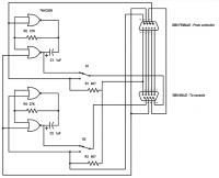
I just had a quick look inside a model 3046 rapid fire unit. It was rather simple so ive drawn it out, which may be useful to some body one day.
|
| |
 
|
- Joined: 25 Feb 2013
- Posts: 384
- Location: Osaka
|
Posted: Tue Apr 07, 2015 3:33 pm
|
|
thank you very much for sharing it!
|
| |
|
- Site Admin
- Joined: 19 Oct 1999
- Posts: 14743
- Location: London
|
Posted: Tue Apr 07, 2015 6:24 pm
|
|
Can an electronics person give us the name for this (astable multivibrator?) and what frequency it operates at for the nominal RC values shown (I failed to figure that out)?
|
| |

|
- Joined: 05 Nov 2014
- Posts: 435
- Location: Auckland - NZ
|
Posted: Wed Apr 08, 2015 12:27 pm
|
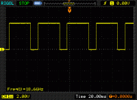
Sounds like a bunch of maths and looking up the NOR gate data sheet to even try and work that out. My scope says 18.66Hz
Do we know how fast you can actually cycle the button inputs before the IO chip is unable to keep up?
|
| |
|
- Joined: 09 Dec 2013
- Posts: 228
- Location: detroit
|
Posted: Wed Apr 08, 2015 1:54 pm
|
wasup wrote Do we know how fast you can actually cycle the button inputs before the IO chip is unable to keep up?
A lot has to do with how certain games process the input, some games work better with slower autofire, others with faster. I know I'm always tweaking the autofire rate on a per-game basis.
best regards,
- dink
|
| |
|
- Site Admin
- Joined: 19 Oct 1999
- Posts: 14743
- Location: London
|
Posted: Wed Apr 08, 2015 1:57 pm
|
Most games will read inputs once per frame, or at their gameplay frame rate (which may vary). I imagine the IO chip response is faster than the Z80 polling time, getting you into the hundreds of kHz if you need it.
It's not a 50% duty cycle and the game will be sampling it so there's a real danger of aliasing. Other systems with multiplexed buttons allow the controller to detect reads and produce an exact rate... 18Hz is almost humanly possible.
|
| |
|
- Joined: 05 Nov 2014
- Posts: 435
- Location: Auckland - NZ
|
Posted: Tue Apr 14, 2015 11:38 am
|
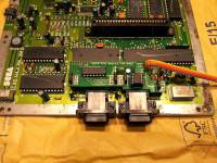
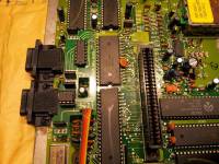
Ive built a nice little auto fire module that drops right into an sms2 if any one is interested to see. Ive remved EM16, EM18, EM26 and EM28, poped some headder pins in and it solders straight in on top. I found a cleaver place to get +5v too, which was the top of a diode that was kind of in the way (not really visable in the pictures), but its on one edge of the cut out in the middle of the board. Ive put a plated edge there to make soldering to it easy. Its got a variable repeat rate between 5 and 25Hz. Buttons A and B are individually selectable and it works on both controller ports. Just need to finish off a front panel for it with some switches and a pot and itll be a nice little mod.
|
| |
|
- Joined: 25 Feb 2013
- Posts: 384
- Location: Osaka
|
Posted: Wed Apr 12, 2017 10:22 am
|
I was having a look at the schematic
For a single button, it looks like this

However, in this way, the top gate will oscillate, with a speed which seems not influenced by C1.
I would expect the schematic to be like this

In this case, the timing would make sense: (27E3*1E-6)*2 = 54ms, 18.51 Hz.
Can you (wasup) or someone else confirm which schematic corresponds to the hardware?
|
| |
|
- Joined: 17 Nov 2015
- Posts: 97
- Location: Canada
|
Posted: Wed Apr 12, 2017 4:24 pm
|
kamillebidan wrote
In this case, the timing would make sense: (27E3*1E-6)*2 = 54ms, 18.51 Hz.
I don't think the second one will work very well unless the gate has some hysteresis (like a schmitt trigger)
The first one it looks like the top gate is drawn backwards. The input should come from the capacitor and the output should drive the other gate. This type of oscillator will have voltages higher and lower than Vcc and Gnd respectively on the output of the capacitor so the logic family has to have input clamping diodes to absorb that. I've seen a resistor in series with the input to that top gate to limit this over/under voltage rush current through the clamping diodes, or at least that's what I think it's for.
An oscillator as described in the last paragraph should have about 50% duty cycle which is not what you see in that scope image.
|
| |
|
- Joined: 14 Mar 2016
- Posts: 58
- Location: Australia
|
Posted: Wed Apr 12, 2017 10:20 pm
|
I know this isn't really a technical response. I recently picked up an official rapid fire unit.
What games would you consider it essential for?
|
| |
|
- Joined: 25 Feb 2013
- Posts: 384
- Location: Osaka
|
Posted: Wed Apr 12, 2017 11:43 pm
|
@Alcoholics Anonymous:
You are completely right, without hysteresis it should start switching around the threshold value. 74hc02n does not have schmitt trigger input, so the second circuit is to exclude.
About your circuit description, do you mean the following circuit?
If so, do inputs have an internal pullup? If not, the following situation would be possible
first gate
upper input 0 (button pushed)
lower input 0
output 1
second gate
upper input 1
output 0
and the circuit would not oscillate
@k4l
fantasy zone
|
| |
|
- Joined: 17 Nov 2015
- Posts: 97
- Location: Canada
|
Posted: Thu Apr 13, 2017 3:57 am
|
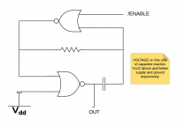
No I mean like the attached.
Most often there is a resistor in series with the input to the top nor gate from the capacitor to limit inrush current when the voltage there suddenly shifts to Vcc/2 below ground or above Vcc.
This oscillator also may not oscillate if the capacitance is too small (unlikely) and in real designs usually there are three inverting gates to ensure oscillation starts.
You'll see this one on the internet quite often usually lacking any informative details and with inverters replacing the nor gates.
|
| |
|
- Joined: 25 Feb 2013
- Posts: 384
- Location: Osaka
|
Posted: Thu Apr 13, 2017 5:21 am
|
I see. now I completely get what you mean: if we call the point at the right of the capacitor A,
when out gets to 1 Va becomes 3/2Vcc, and is discharged by the resistor (which is now pulling to ground). When Va is drops under vcc/2, out goes to 0, and Va becomes -1/2Vcc, and the resistor pulls up, isn't it?
|
| |
|
- Joined: 17 Nov 2015
- Posts: 97
- Location: Canada
|
Posted: Thu Apr 13, 2017 4:32 pm
|
Yes that's it. There will be clamping diodes at the input of the top nor gate that will immediately drop the Vcc*3/2 high voltage to Vcc and raise the -Vcc/2 low voltage to 0 (within a Vbe drop of course). Depending on the capacitance that can be a lot of charge that is drained quickly so that's why there is usually a resistor in series with the input to the top nor gate. The clamping diodes mean the swing is always from 0 to Vcc/2 or Vcc to Vcc/2 before switching happens.
Since the voltage swing is symmetrical there should be a 50% duty cycle waveform but the voltage trace shown above is not 50%. I'm thinking that's a simulation of the originally misdrawn circuit (rather than a measurement) or if the designers actually made the mistake and the wrong circuit is in there for real.
|
| |
|